


MuxOneNAND2G(KFM2G16Q2A-DEBx)
- 103 -
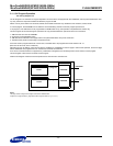
FLASH MEMORY
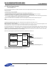
MuxOneNAND4G(KFN4G16Q2A-DEBx)
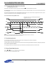
3.9.5 Handshaking Operation During Synchronous Burst Block Read Mode
The handshaking feature allows the host system to simply monitor the RDY signal from the device to determine when the initial word of burst
data is ready to be read.
To set the number of initial cycles for optimal burst mode, the host should use the programmable burst read latency configuration (see Section
2.8.19, "System Configuration1 Register").
The rising edge of RDY which is derived at the same cycle of data fetch clock indicates the initial word of valid burst data.
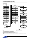
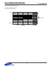
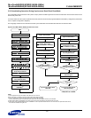
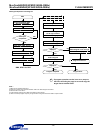
Synchronous Burst Block Read Operation Flow Chart
NOTE :
1) These registers must be set as BSA=1000, BSC=00 and FSA=00.
2) INT auto mode is mandatory for Synchronous Burst Block Read Operation.
3) For the continuous synchronous burst block read, only INT PIN is availabe.
For the other fixed number of words linear burst block read, both INT register and INT pin are avilable.
4) While reading data from DataRAM, all normal synchronous burst read mode is supported for the main area.
5) At this time, host should disable the CE of OneNAND in order to operate another device. Even if host does not operate another device,
CE should be disabled during INT low.
Write ‘DFS, FBA’ of Flash
Add: F100h DQ=DFS*, FBA
Start
Write ‘FPA, FSA’ of Flash
Add: F107h DQ=FPA, FSA
1)
Write ‘FPC’ of Flash
Add: F104h DQ=FPC
Write Synchronous Burst
Add=F220h DQ=000Ah
Block Read Command
Wait for INT register or PIN
3)
low to high transition
Add: F241h DQ[15]=INT
Host reads data from
DataRAM 0
4)
Wait for INT register or PIN
3)
high to low transition
Add: F241h DQ[15]=INT
Host may operate
another device while
CE
of OneNAND is disabled
5)
Wait for INT register or PIN
3)
low to high transition
Add: F241h DQ[15]=INT
Wait for INT register or PIN
3)
high to low transition
Add: F241h DQ[15]=INT
Host may operate
another device while
CE
of OneNAND is disabled
5)
Wait for INT register or PIN
3)
low to high transition
Add: F241h DQ[15]=INT
Finished reading
final page set by FPC?
YES
Read Controller
Status Register
Add: F240h DQ[10]=1(Error)
Synchronous Burst Block
DQ[10]=0?
YES
NO
Read Completed
Synchronous Burst Block
Read Fail
NO
Finished reading
final page set by FPC?
YES
Host reads data from
DataRAM 1
4)
Host reads data from
DataRAM 0
4)
NO
Write ‘BSA’, ‘BSC’ of Flash
1)
Add: F200h DQ=BSA, BSC
Select DataRAM for DDP
Add: F101h DQ=DBS*
* DBS, DFS is for DDP
Write 0 to INT register or PIN
2)3)
Add: F241h DQ=0000h