


MuxOneNAND2G(KFM2G16Q2A-DEBx)
- 116 -
FLASH MEMORY
MuxOneNAND4G(KFN4G16Q2A-DEBx)
3.13 Erase Operation
There are multiple methods for erasing data in the device including Block Erase and Multi-Block Erase.
3.13.1 Block Erase Operation
See Timing Diagram 6.16
The Block Erase Operation is done on a block basis. To erase a block is to write all 1's into the desired memory block by executing the Internal
Erase Routine. All previous data is lost.
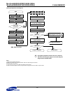
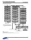
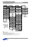
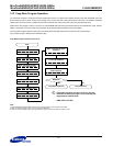
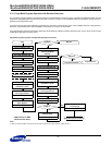
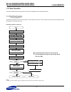
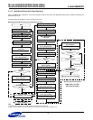
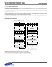
Block Erase Operation Flow Chart
NOTE :
1) ‘Write 0 to interrupt register’ step may be ignored when using INT auto mode. Refer to chapter 2.8.18.1.
Start
Write ‘DFS*, FBA’ of Flash
Add: F100h DQ=DFS*, FBA
Write ‘Erase’ Command
Add: F220h DQ=0094h
Wait for INT register
Add: F241h DQ=[15]=INT
low to high transition
: If erase operation results in an error, map out
the failing block and replace it with another block.
*
Write 0 to interrupt register
1)
Add: F241h DQ=0000h
* DFS is for DDP
Select DataRAM for DDP
Add: F101h DQ=DBS*
Read Interrupt register
Add: F241h DQ[5]=EI
DQ[5]=1?
YES
Add: F240h DQ[10]=Error
Read Controller
Status Register
Erase completed
DQ[10]=0?
YES
Erase Error
NO
Add: F240h DQ[14]=Lock
Read Controller
Status Register ‘Lock’ bit high
Erase Lock Error
NO