


MuxOneNAND2G(KFM2G16Q2A-DEBx)
- 48 -
FLASH MEMORY
MuxOneNAND4G(KFN4G16Q2A-DEBx)
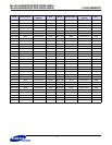
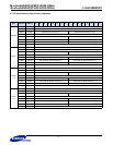
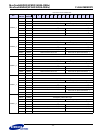
2.7.2 lnternal Memory Spare Area Assignment
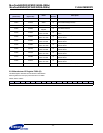
The figure below shows the assignment of the spare area in the Internal Memory NAND Array.
Spare Area Assignment in the Internal Memory NAND Array Information
NOTE 5 :
In case of ECC Bypass Mode, user can program in ECC Area.
NOTE 6 :
For all blocks, 8th word is available to the user.
However,in case of OTP Block, 8th word of sector 0, page 0 is reserved as OTP Locking Bit area.
Therefore, in case of OTP Block, user usage on this area is prohibited.
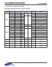
Word Byte Note Description
1
LSB
1 Invalid Block information in 1st and 2nd page of an invalid block
MSB
2
LSB
2 Managed by internal ECC logic for Logical Sector Number dataMSB
3
LSB
MSB
3 Reserved for future use
4
LSB
MSB
5
LSB
Dedicated to internal ECC logic. Read Only. (Note 5)
ECCm 1st for main area data
MSB
Dedicated to internal ECC logic. Read Only. (Note 5)
ECCm 2nd for main area data
6
LSB
Dedicated to internal ECC logic. Read Only. (Note 5)
ECCm 3rd for main area data
MSB
Dedicated to internal ECC logic. Read Only. (Note 5)
ECCs 1st for 2nd word of spare area data
7
LSB
Dedicated to internal ECC logic. Read Only. (Note 5)
ECCs 2nd for 3rd word of spare area data
MSB 3 Reserved for future use
8
LSB
4 Available to the user (Note 6)
MSB
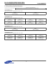
Main area
256W
Main area
256W
Main area
256W
Main area
256W
Spare
area
8W
Spare
area
8W
Spare
area
8W
Spare
area
8W
1
st
W
ECCm
1st
ECCm
2nd
ECCm
3rd
ECCs
1st
ECCs
2nd
LSB MSB
LSB MSB
2
nd
W
LSB MSB
3
rd
W
LSB MSB
4
th
W
LSB MSB
5
th
W
LSB MSB
6
th
W
LSB MSB
7
th
W
LSB MSB
8
th
W
LSB MSB
Note1 Note1 Note2 Note2 Note2 Note3 Note3 Note3 Note4 Note4
Note3