


MuxOneNAND2G(KFM2G16Q2A-DEBx)
- 82 -
FLASH MEMORY
MuxOneNAND4G(KFN4G16Q2A-DEBx)
3.0 DEVICE OPERATION
This section of the datasheet discusses the operation of the MuxOneNAND device. It is followed by AC/DC
Characteristics and Timing Diagrams which may be consulted for further information.
The MuxOneNAND supports a limited command-based interface in addition to a register-based interface for performing operations on the
device.
3.1 Command Based Operation
The command-based interface is active in the boot partition. Commands can only be written with a boot area address. Boot area data is only
returned if no command has been issued prior to the read.
The entire address range, except for the boot area, can be used for the data buffer. All commands are written to the boot partition. Writes out-
side the boot partition are treated as normal writes to the buffers or registers.
The command consists of one or more cycles depending on the command. After completion of the command the device starts its execution.
Writing incorrect information including address and data to the boot partition or writing an improper command will terminate the previous com-
mand sequence and make the device enter the ready status.
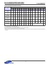
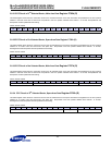
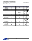
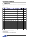
The defined valid command sequences are stated in Command Sequences Table.
Command based operations are mainly used when MuxOneNAND is used as Booting device, and all command based operations only sup-
ports asynchronous reads and writes. With DDP, command based operation except reset is applicable only on chip1.
Command Sequences
NOTE :
1) BP(Boot Partition) : BootRAM Area [0000h ~ 01FFh, 8000h ~ 800Fh]. (Chip 1 only in case of DDP)
2) Load Data into Buffer operation is available within a block(128KB) (Chip1 only in case of DDP)
3) Load 2KB unit into DataRAM0. Current Start address(FPA) is automatically incremented by 2KB unit after the load.
4) 0000h -> Data is Manufacturer ID (Chip1 only in case of DDP)
0001h -> Data is Device ID (Chip1 only in case of DDP)
0002h -> Current Block Write Protection Status (Chip1 only in case of DDP)
5) WE
toggling can terminate ‘Read Identification Data’ operation.
Command Definition Cycles 1st cycle 2nd cycle
Reset MuxOneNAND
Add
1
BP
1)
Data 00F0h
Load Data into Buffer
2)
Add
2
BP BP
Data 00E0h
0000h
3)
Read Identification Data
5)
Add
2
BP
XXXXh
4)
Data 0090h Data