


MuxOneNAND2G(KFM2G16Q2A-DEBx)
- 113 -
FLASH MEMORY
MuxOneNAND4G(KFN4G16Q2A-DEBx)
3.12 Copy-Back Program Operation
The Copy-Back program is configured to quickly rewrite data stored in one page without utilizing memory other than OneNAND. Since the
time-consuming cycles of serial access and re-loading cycles are removed, the system performance is improved. The benefit is especially
obvious when a portion of block is updated and the rest of the block also need to be copied to the newly assigned free block.
Data from the source page is saved in one of the on-chip DataRAM buffers and then programmed directly into the destination page. The Dat-
aRAM is overwritten the previous data using the Buffer Sector Address (BSA) and Buffer Sector Count (BSC).
The Copy-Back Program Operation does this by performing sequential page-reads without a serial access and executing a
copy-program using the address of the destination page.
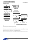
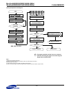
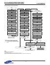
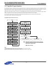
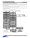
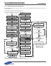
Copy-Back Program Operation Flow Chart
NOTE :
1) Selected DataRAM by BSA & BSC is used for Copy back operation, so previous data is overwritten.
2) FBA, FPA and FSA should be input prior to FCBA, FCPA and FCSA.
3) ’Write 0 to interrupt register’ step may be ignored when using INT auto mode. Refer to chapter 2.8.18.1.
Start
Write ’DFS, FBA’ of Flash
Add: F100h DQ=DFS, FBA
Write ’FPA, FSA’ of Flash
Add: F107h DQ=FPA, FSA
Write ’FCBA’ of Flash
Add: F102h DQ=FCBA
Write ’FCPA, FCSA’ of Flash
Add: F103h DQ=FCPA, FCSA
Copy back completed
Write ’Copy-back Program’
command
Add: F220h DQ=001Bh
Wait for INT register
low to high transition
Add: F241h DQ[15]=INT
Read Controller
Status Register
Add: F240h DQ[10]=Error
DQ[10]=0?
Copy back Error
YES NO
: If program operation results in an error, map out
the block including the page in error and copy the
target data to another block.
*
Write 0 to interrupt register
Add: F241h DQ=0000h
Write ’BSA, BSC’ of DataRAM
Add: F200h DQ=BSA, BSC
1)
Select DataRAM for DDP
Add: F101h DQ=DBS
* DBS, DFS is for DDP