


MuxOneNAND2G(KFM2G16Q2A-DEBx)
- 164 -
FLASH MEMORY
MuxOneNAND4G(KFN4G16Q2A-DEBx)
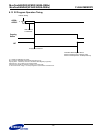
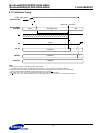
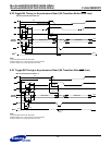
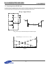
6.22 Toggle Bit Timing in Asynchronous Read (VA Transition Before AVD Low)
See AC Characteristics Table 5.5
NOTE :
1) VA=Valid Read Address, RD=Read Data.
2) Before IOBE is set to 1, RDY and INT pin are High-Z state.
3) Refer to chapter 5.5 for tASO description and value.
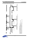
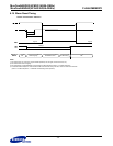
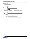
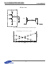
6.23 Toggle Bit Timing in Asynchronous Read (VA Transition After AVD Low)
See AC Characteristics Table 5.5
NOTE :
1) VA=Valid Read Address, RD=Read Data.
2) Before IOBE is set to 1, RDY and INT pin are High-Z state.
3) Refer to chapter 5.5 for tASO description and value.
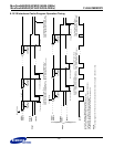
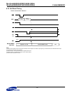
tOE
Status RD
1)
tCE
tOEZ
tAVDP
CE
OE
WE
A/DQ0:
AVD
A/DQ15
Hi-Z
RDY
2)
tAA
tRC
tCA
tCEZ
tCER
tAVDO
Hi-Z
VA Status RD
Hi-Z
tASO
tAAVDH
tAAVDS
VA
1)
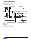
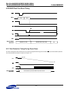
tOE
Status RD
1)
tOEZ
tACC
tAAVDH
tAVDP
tAAVDS
CE
OE
WE
A/DQ0:
AVD
A/DQ15
tCEZ
tCA
tCER
tAVDO
Hi-Z
Hi-Z
RDY
2)
tRC
tCE
Hi-Z
VA
Status RD
tCA
tASO
VA
1)