


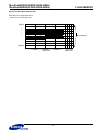
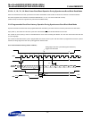

MuxOneNAND2G(KFM2G16Q2A-DEBx)
- 108 -
FLASH MEMORY
MuxOneNAND4G(KFN4G16Q2A-DEBx)
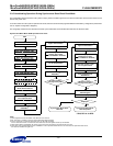
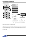
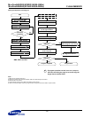
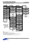
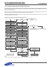
2X Program Operation Flow Diagram
NOTE :
1) DBS must be set before data input.
2) Data input could be done anywhere between "Start" and "Write Program Command"
3) FBA must be an even block.
4)
These registers must be set as BSA=1000, BSC=00 and FSA=00.
5) ‘Write 0 to interrupt register’ step may be ignored when using INT auto mode. Refer to chapter 2.8.18.1
Start
Data Input
Write ‘DFS*, FBA’ of Flash
Add: F100h DQ=DFS*, FBA
3)
Write ‘FPA, FSA’ of Flash
Add: F107h DQ=FPA, FSA
4)
Select DataRAM for DDP
1)
Add: F101h DQ=DBS*
Write Data into DataRAM
2)
ADD: DP DQ=Data-in
Write ‘2X Program’ Command
Completed?
Wait for INT register
low to high transition
Add: F241h DQ[15]=INT
NO
YES
* DBS, DFS is for DDP
: If program operation results in an error, map out
the block including the page in error and copy the
target data to another block.
*
Write 0 to interrupt register
5)
Add: F241h DQ=0000h
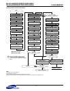
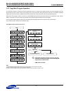
Write ‘BSA, BSC’ of DataRAM
4)
Add: F200h DQ=BSA, BSC
Add: F220h DQ=007Dh
Read Interrupt register
Add: F241h DQ[6]=WI
DQ[6]=1?
YES
Add: F240h DQ[10]=Error
Read Controller
Status Register
Program completed
DQ[10]=0?
YES
Program Error
NO
NO
Add: F240h DQ[14]=Lock
Read Controller
Status Register ‘Lock’ bit high
Program Lock Error