


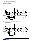
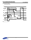
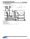

MuxOneNAND2G(KFM2G16Q2A-DEBx)
- 147 -
FLASH MEMORY
MuxOneNAND4G(KFN4G16Q2A-DEBx)
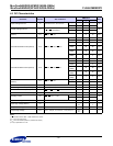
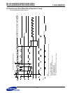
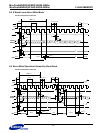
6.3 Synchronous Burst Block Read Operation Timing
See AC Characteristics table 5.4 and 5.7.
WE
CE
CLK
tDS
tWPL
tCS
tWPH
tWC
AA
FPAFBA
AA
ADQ0-
OE
tAAVDH
tAAVDS
INT
tCH
tCS
AVD
V
IL
tDH
tRD2
CA
SBBRCDFPC
AA
ADQ15
Hi-Z
D0 D1 D2
RDY
NOTE :
Asynchronous write was used in this timing diagram. Synchronous write is also possible.
1. AA = Address of address register
CA = Address of command register
SBBRCD = Synchronous Burst Block Read Command
FBA = Flash Block Address
FPA = Flash Page Address
BSA = BufferRAM Sector Address
FPC= Number of Flash Page to be read (3pages ~ 64pages)
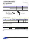
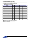
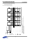
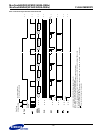
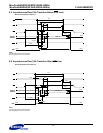
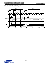
Synchronous Burst Block Read Command Sequence
. . .
. . .
. . .
. . .
. . .
. . .
. . .
. . .
Start Add
BSA
AA