


MuxOneNAND2G(KFM2G16Q2A-DEBx)
- 92 -
FLASH MEMORY
MuxOneNAND4G(KFN4G16Q2A-DEBx)
3.5 Data Protection During Power Down Operation
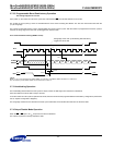
See Timing Diagram 6.21
The device is designed to offer protection from any involuntary program/erase during power-transitions.
RP
pin which provides hardware protection is recommended to be kept at VIL before Vcc drops to 1.5V.
3.6 Load Operation
See Timing Diagrams 6.11
The Load operation is initiated by setting up the start address from which the data is to be loaded. The Load command is issued in order to ini-
tiate the load.
During a Load operation, the device:
-Transfers the data from NAND Flash array into the BufferRAM
-ECC is checked and any detected and corrected error is reported in the status response as well as
any unrecoverable error.
Once the BufferRAM has been filled, an interrupt is issued to the host so that the contents of the BufferRAM can be read. The read from the
BufferRAM can be an asynchronous read mode or synchronous read mode. The status information related to load operation can be checked
by the host if required.
The device has a dual data buffer memory architecture (DataRAM0, DataRAM1), each 2KB in size. Each DataRAM buffer has 4
Sectors. The device is capable of independent and simultaneous data-read operation from one data buffer and data-load operation to the
other data buffer. Refer to the information for more details in section 3.15.1, "Read-While-Load Operation".
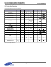
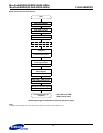
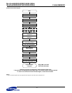
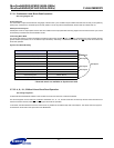
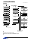
Load Operation Flow Chart Diagram
NOTE :
1) ‘Write 0 to interrupt register’ step may be ignored when using INT auto mode. Refer to chapter 2.8.18.1
Start
Write ‘DFS*, FBA’ of Flash
Add: F100h DQ=DFS, FBA
Write ‘FPA, FSA’ of Flash
Add: F107h DQ=FPA, FSA
Write ‘BSA, BSC’ of DataRAM
Add: F200h DQ=BSA, BSC
Select DataRAM for DDP
Add: F101h DQ=DBS
Write ‘Load’ Command
Add: F220h
DQ=0000h or 0013h
Wait for INT register
low to high transition
Add: F241h DQ[15]=INT
Read Controller
Add: F240h DQ[10]=Error
DQ[10]=0?
NO
YES
* DBS, DFS is for DDP
Status Register
Host reads data from
DataRAM
Read completed
Map Out
Write 0 to interrupt register
1)
Add: F241h DQ=0000h