


MuxOneNAND2G(KFM2G16Q2A-DEBx)
- 59 -
FLASH MEMORY
MuxOneNAND4G(KFN4G16Q2A-DEBx)
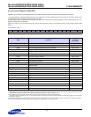
2.8.9 Start Address1 Register F100h (R/W)
This Read/Write register describes the NAND Flash block address which will be loaded, programmed, or erased.
F100h, default = 0000h
NOTE :
1) Bit 0 should be fixed ‘low’ at 2X Program and 2X Cache Program.
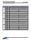
Start Address1 Information
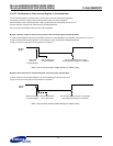
2.8.10 Start Address2 Register F101h (R/W)
This Read/Write register describes the BufferRAM of DDP (Device BufferRAM Select)
F101h, default = 0000h
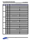
Start Address2 Information
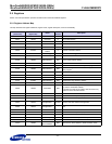
In the case of writing Register, both registers in chip1 and chip2 will be written regardless of DBS. Reading out from Register of chip1/chip2
follows the DBS setting.
In using DDP chip, BootRAM of Chip 1 will always be selected regardless of DBS.
Reading and Writing on the DataRAM of DDP chip is different. Only the DataRAM selected by DBS will be written and read out.
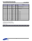
15 14 13 12 11 10 9 8 7 6 5 4 3 2 1 0
DFS Reserved(0000)
FBA
1)
Device Number of Block FBA
2Gb 2048 FBA[10:0]
4Gb DDP 4096 DFS[15] & FBA[10:0]
Register Information Description
FBA NAND Flash Block Address
DFS Flash Core of DDP (Device Flash Core Select)
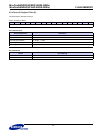
15 14 13 12 11 10 9 8 7 6 5 4 3 2 1 0
DBS Reserved(000000000000000)
Register Information Description
DBS BufferRAM and Register of DDP (Device BufferRAM Select)
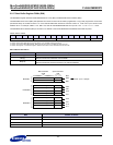
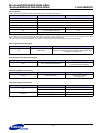
Comp
Comp
DBS
DFS
DDP_OPT
GND
CE
CONTROL
LOGIC
SRAM
BUFFER
FLASH
CORE
Comp
Comp
DBS
DFS
DDP_OPT
V
DD
CE
CONTROL
LOGIC
SRAM
BUFFER
FLASH
CORE
CE INT
CHIP 1
CHIP 2
INT
INT
*Comp = Comparator