


MuxOneNAND2G(KFM2G16Q2A-DEBx)
- 90 -
FLASH MEMORY
MuxOneNAND4G(KFN4G16Q2A-DEBx)
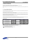
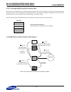
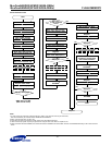
Data Protection Operation Flow Diagram
* Samsung strongly recommends to follow the above flow chart
NOTE :
1) ‘Write 0 to interrupt register’ step may be ignored when using INT auto mode. Refer to chapter 2.8.18.1
* DFS, DBS is for DDP
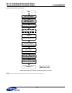
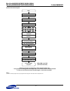
Start
Lock/Unlock/Lock-Tight
Write ‘lock/unlock/lock-tight’
Add: F220h
DQ=002Ah/0023h/002Ch
Wait for INT register
low to high transition
Add: F241h DQ[15]=INT
Write 0 to interrupt register
1)
Add: F241h DQ=0000h
Command
completed
Write ‘DFS*’, of Flash
Add: F100h DQ=DFS*
Write ‘SBA’ of Flash
Add: F24Ch DQ=SBA
Select DataRAM for DDP
Add: F101h DQ=DBS*
Add: F240h DQ[10]=0(pass)
Read Controller
Status Register
Add: F24Eh DQ[2:0]=US,LS,LTS
Read Write Protection Register
Write ’DFS*’, ’FBA’ of Flash
Add: F100h DQ=DFS, FBA
(DFS must be same)