


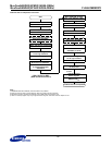
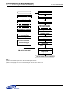

MuxOneNAND2G(KFM2G16Q2A-DEBx)
- 124 -
FLASH MEMORY
MuxOneNAND4G(KFN4G16Q2A-DEBx)
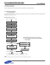
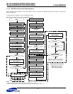
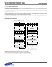
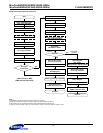
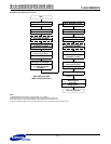
OTP Block Program Operation Flow Chart
NOTE :
1) FBA(NAND Flash Block Address) could be omitted or any address.
2) Data input could be done anywhere between "Start" and "Write Program Command".
3) FBA should point the unlocked area address among NAND Flash Array address map.
4) ‘Write 0 to interrupt register’ step may be ignored when using INT auto mode. Refer to chapter 2.8.18.1.
Select DataRAM for DDP
Add: F101h DQ=DBS*
Write ‘DFS*, FBA’ of Flash
1)
Add: F100h DQ=DFS*, FBA
Start
Data Input
Write ‘OTP Access’ Command
Add: F220h DQ=0065h
Write ‘FPA, FSA’ of Flash
Add: F107h DQ=FPA, FSA
Write ‘BSA, BSC’ of DataRAM
Add: F200h DQ=BSA, BSC
Write Data into DataRAM
2)
Add: DP DQ=Data-in
OTP Programming completed
Write Program command
DQ=0080h or 001Ah
Completed?
Wait for INT register
low to high transition
Add: F241h DQ[15]=INT
NO
Add: F220h
Wait for INT register
Add: F241h DQ[15]=INT
Write 0 to interrupt register
4)
Add: F241h DQ=0000h
low to high transition
Do Cold/Warm/Hot
OTP Exit
Automatically
checked
Wait for INT register
low to high transition
Add: F241h DQ[15]=INT
OTP Exit
Automatically
OTPL=0?
YES
NO
updated
Read Controller
Status Register
Add: F240h DQ[10]=1(Error)
Add: F200h DQ=BSA, BSC
Write ‘DFS, FBA’ of Flash
Add: F100h DQ=DFS, FBA
3)
Read Controller
Status Register
Add: F240h DQ[10]=0(Pass)
/NAND Flash Core reset
Do Cold/Warm/Hot
/NAND Flash Core reset
Write 0 to interrupt register
4)
Add: F241h DQ=0000h
* DBS, DFS is for DDP
Update Controller
Add: F240h
Status Register
DQ[14]=1(Lock), DQ[10]=1(Error)
(DBS and DFS must be 0)