


MuxOneNAND2G(KFM2G16Q2A-DEBx)
- 122 -
FLASH MEMORY
MuxOneNAND4G(KFN4G16Q2A-DEBx)
3.14.1 OTP Block Load Operation
An OTP Block Load Operation accesses the OTP area and transfers identified content from the OTP to the DataRAM on-chip buffer, thus
making the OTP contents available to the Host.
The OTP area is a separate part of the NAND Flash Array memory. It is accessed by issuing OTP Access command(65h) instead of a Flash
Block Address (FBA) command.
After being accessed with the OTP Access Command, the contents of OTP memory area are loaded using the same operations as a normal
load operation to the NAND Flash Array memory (see section 3.6 for more information).
To exit the OTP access mode following an OTP Block Load Operation, a Cold-, Warm-, Hot-, or NAND Flash Core Reset operation is per-
formed.
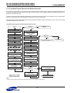
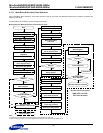
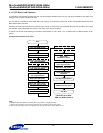
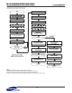
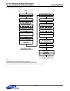
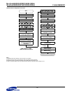
OTP Block Read Operation Flow Chart
NOTE :
1) FBA(NAND Flash Block Address) could be omitted or any address in a single die package.
FBA must be an address of a chip containing OTP block that is supposed to be accessed in DDP
2) ‘Write 0 to interrupt register’ step may be ignored when using INT auto mode. Refer to chapter 2.8.18.1.
Start
Wait for INT register
Add: F241h DQ[15]=INT
Write 0 to interrupt register
2)
Add: F241h DQ=0000h
Write ‘FPA, FSA’ of Flash
Add: F107h DQ=FPA, FSA
OTP Reading completed
Write ‘Load’ Command
Add: F220h
DQ=0000h or 0013h
Wait for INT register
low to high transition
Add: F241h DQ[15]=INT
Write ‘OTP Access’ Command
Add: F220h DQ=0065h
Write ‘BSA, BSC’ of DataRAM
Add: F200h DQ=BSA, BSC
low to high transition
OTP Exit
Host reads data from
DataRAM
Do Cold/Warm/Hot
/NAND Flash Core Reset
Write ‘DFS*, FBA’ of Flash
1)
Add: F100h DQ=DFS*, FBA
Write 0 to interrupt register
2)
Add: F241h DQ=0000h
Select DataRAM for DDP
Add: F101h DQ=DBS*
* DBS, DFS is for DDP
(DBS and DFS must be 0)