


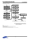

MuxOneNAND2G(KFM2G16Q2A-DEBx)
- 112 -
FLASH MEMORY
MuxOneNAND4G(KFN4G16Q2A-DEBx)
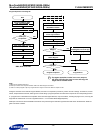
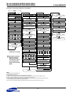
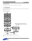
2X Interleave Cache Program Operation Flow Diagram
NOTE :
1) DBS must be set before data input.
2) FBA must be an even block.
3)
These registers must be set as BSA=1000, BSC=00 and FSA=00.
4)
‘Write 0 to interrupt register’ step may be ignored when using INT auto mode. Refer to chapter 2.8.18.1
.
5) Host is strongly recommended to see the INT register(F241h) of each chip.
6) Once ‘2X PGM command’ is issued onto a chip, the same command(2X PGM) must be issued onto another chip.
If not, Samsung can not gurantee the following operation.
7) If error bit is set at this step, DQ[1]~[4] shoulde be checked in order to find where the error occurred.
Start
Write ’DFS, FBA’ of Flash
Add: F100h DQ=DFS, FBA
2)
Select DataRAM for DDP
1)
Add: F101h DQ=DBS
Check INT register
Add: F241h DQ=8040h
complete
Map Out
if it is ready
5)
Write ’FPA, FSA’ of Flash
Add: F107h DQ=FPA, FSA
3)
Write ’BSA’, ’BSC’ of Flash
3)
Add: F200h DQ=BSA, BSC
Write Data into DataRAM0,1
Add: DataRAM DQ=Data(4KB)
Write 2X Cache PGM CMD
Add: F220h DQ=007Fh
Add: F240h
Read Controller
Status Register
Is it first input
for a chip
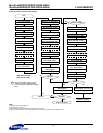
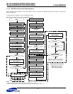
Select DataRAM for DDP
1)
Add: F101h DQ=DBS
DQ[4] | DQ[2] = 0?
Last 2 Plane PGM
for a chip?
Write ’DFS, FBA’ of Flash
Add: F100h DQ=DFS, FBA
2)
Write ’FPA, FSA’ of Flash
Add: F107h DQ=FPA, FSA
3)
Write ’BSA’, ’BSC’ of Flash
3)
Add: F200h DQ=BSA, BSC
Write Data into DataRAM0,1
Add: DataRAM DQ=Data(4KB)
Write 2X PGM CMD
6)
Add: F220h DQ=007Dh
Write ’DFS, FBA’ of Flash
Add: F100h DQ=DFS, FBA
2)
Write ’FPA, FSA’ of Flash
Add: F107h DQ=FPA, FSA
3)
Write ’BSA’, ’BSC’ of Flash
3)
Add: F200h DQ=BSA, BSC
Write Data into DataRAM0,1
Add: DataRAM DQ=Data(4KB)
Write 2X PGM CMD
6)
Add: F220h DQ=007Dh
Select DataRAM for DDP
1)
Add: F101h DQ=DBS
Check INT register
Add: F241h DQ=8040h
if it is ready
5)
DQ[4] | DQ[2] = 0?
DQ[10]=0?
Wait for INT register
Add: F241h DQ=8040h
low to high transition
4)
Add: F240h DQ[10]=Error
Read Controller
Status Register
7)
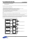
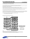
Select DataRAM for DDP
1)
Add: F101h DQ=DBS
Check INT register
Add: F241h DQ=8040h
if it is ready
5)
DQ[10]=0?
Add: F240h DQ[10]=Error
Read Controller
Status Register
7)
YES
NO
YES
YES
NO
NO
YES
NO
YES
NO
YES
NO
* DBS, DFS is for DDP
*
If program operation
results in an error,
map out the block
including the page in
error and copy the
target data to another
block.
DQ[4],[2]=Plane1,2 previous
Add: F240h
Read Controller
Status Register
DQ[4],[2]=Plane1,2 previous
Write 0 to Interrupt register
4)
Add: F241h DQ=0000h
Write 0 to Interrupt register
4)
Add: F241h DQ=0000h
Write 0 to Interrupt register
4)
Add: F241h DQ=0000h