


MuxOneNAND2G(KFM2G16Q2A-DEBx)
- 105 -
FLASH MEMORY
MuxOneNAND4G(KFN4G16Q2A-DEBx)
3.11 Program Operation
See Timing Diagram 6.12
The Program operation is used to program data from the on-chip BufferRAMs into the NAND FLASH memory array.
The device has two 2KB data buffers, each 1 Page (2KB + 64B) in size. Each page has 4 sectors of 512B each main area and 16B spare area.
The device can be programmed in units of 1~4 sectors.
The architecture of the DataRAMs permits a simultaneous data-write operation from the Host to one of data buffers and a program operation
from the other data buffer to the NAND Flash Array memory. Refer to Section 3.15.2, "Write While Program Operation", for more information.
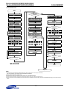
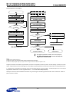
Addressing for program operation
Within a block, the pages must be programmed consecutively from the LSB (least significant bit) page of the block to MSB (most significant
bit) pages of the block. Random page address programming is prohibited.
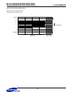
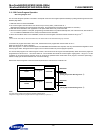
From the LSB page to MSB page
DATA IN: Data (1)
Data (64)
(1)
(2)
(3)
(32)
(64)
Data register
Page 0
Page 1
Page 2
Page 31
Page 63
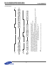
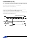
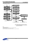
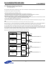
Ex.) Random page program (Prohibition)
DATA IN: Data (1)
Data (64)
(2)
(32)
(3)
(1)
(64)
Data register
Page 0
Page 1
Page 2
Page 31
Page 63
:
:
:
: