


MuxOneNAND2G(KFM2G16Q2A-DEBx)
- 136 -
FLASH MEMORY
MuxOneNAND4G(KFN4G16Q2A-DEBx)
3.18 Invalid Block Operation
Invalid blocks are defined as blocks in the device's NAND Flash Array memory that contain one or more invalid bits whose reliability is not
guaranteed by Samsung.
The information regarding the invalid block(s) is called the Invalid Block Information. Devices with invalid block(s) have the same quality level
as devices with all valid blocks and have the same AC and DC characteristics.
An invalid block(s) does not affect the performance of valid block(s) because it is isolated from the bit line and the common source line by a
select transistor.
The system design must be able to mask out the invalid block(s) via address mapping. The 1st block, which is placed on 00h block address, is
always fully guaranteed to be a valid block.
Due to invalid marking, during load operation for identifying invalid block, a load error may occur.
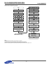
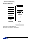
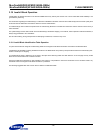
3.18.1 Invalid Block Identification Table Operation
A system must be able to recognize invalid block(s) based on the original invalid block information and create an invalid block table.
Invalid blocks are identified by erasing all address locations in the NAND Flash Array memory except locations where the invalid block(s) infor-
mation is written prior to shipping.
An invalid block(s) status is defined by the 1st word in the spare area. Samsung makes sure that either the 1st or 2nd page of every invalid
block has non-FFFFh data at the 1st word of sector0.
Since the invalid block information is also erasable in most cases, it is impossible to recover the information once it has been erased. Any
intentional erase of the original invalid block information is prohibited.
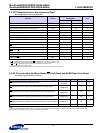
The following suggested flow chart can be used to create an Invalid Block Table.