


Two Port 10/100 Managed Ethernet Switch with 16-Bit Non-PCI CPU Interface
Datasheet
SMSC LAN9311/LAN9311i 143 Revision 1.4 (08-19-08)
DATASHEET
10.2.2.3 I
2
C EEPROM Byte Read
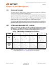
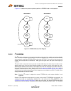
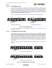
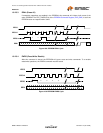
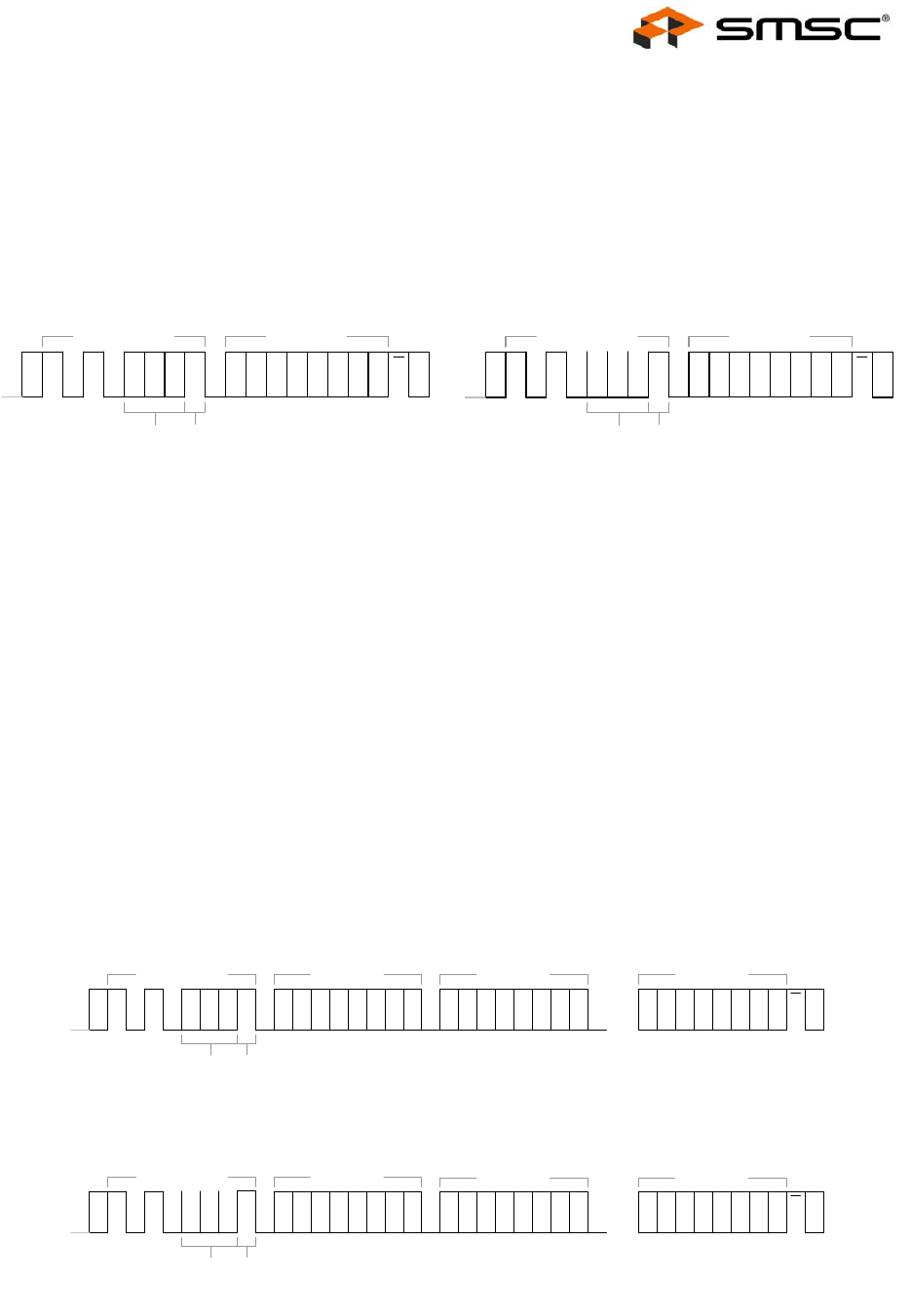
Following the device addressing, a data byte may be read from the EEPROM by outputting a start
condition and control byte with a control code of 1010b, chip/block select bits as described in
Section 10.2.2.2, and the R/~W bit high. The EEPROM will respond with an acknowledge, followed by
8-bits of data. If the EEPROM slave fails to send an acknowledge, then the sequence is aborted and
the EPC_TIMEOUT bit in the EEPROM Command Register (E2P_CMD) is set. The I
2
C master then
sends a no-acknowledge, followed by a stop condition.
Figure 10.4 illustrates typical I
2
C EEPROM byte read for single and double byte addressing.
For a register level description of a read operation, refer to Section 10.2.1, "EEPROM Controller
Operation," on page 139.
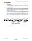
10.2.2.4 I
2
C EEPROM Sequential Byte Reads
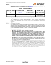
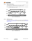
Following the device addressing, data bytes may be read sequentially from the EEPROM by outputting
a start condition and control byte with a control code of 1010b, chip/block select bits as described in
Section 10.2.2.2, and the R/~W bit high. The EEPROM will respond with an acknowledge, followed by
8-bits of data. If the EEPROM slave fails to send an acknowledge, then the sequence is aborted and
the EPC_TIMEOUT bit in the EEPROM Command Register (E2P_CMD) is set. The I
2
C master then
sends an acknowledge, and the EEPROM responds with the next 8-bits of data. This continues until
the last desired byte is read, at which point the I
2
C master sends a no-acknowledge, followed by a
stop condition.
Figure 10.4 illustrates typical I
2
C EEPROM sequential byte reads for single and double byte
addressing.
Figure 10.4 I
2
C EEPROM Byte Read
Figure 10.5 I
2
C EEPROM Sequential Byte Reads
S 1 0 1 0
A
1
0
A
9
A
8
Control Byte
A
C
K
S 1 0 1 0
Control Byte
A
C
K
Single Byte Addressing Read Double Byte Addressing Read
0 0 01
Data Byte
D
7
D
6
D
5
D
4
D
3
D
2
D
1
D
0
A
C
K
P 1
Data Byte
D
7
D
6
D
5
D
4
D
3
D
2
D
1
D
0
A
C
K
P
A
C
K
A
C
K
R/~W
Chip / Block
Select Bits
R/~W
Chip / Block
Select Bits
S 1 0 1 0
A
1
0
A
9
A
8
Control Byte
A
C
K
S 1 0 1 0
Control Byte
A
C
K
Single Byte Addressing Sequential Reads
0 0 0
1
Data Byte
D
7
D
6
D
5
D
4
D
3
D
2
D
1
D
0
A
C
K
P
1
Data Byte
D
7
D
6
D
5
D
4
D
3
D
2
D
1
D
0
A
C
K
A
C
K
A
C
K
Data Byte
D
7
D
6
D
5
D
4
D
3
D
2
D
1
D
0
A
C
K
Data Byte
D
7
D
6
D
5
D
4
D
3
D
2
D
1
D
0
A
C
K
P
A
C
K
Data Byte
D
7
D
6
D
5
D
4
D
3
D
2
D
1
D
0
A
C
K
Data Byte
D
7
D
6
D
5
D
4
D
3
D
2
D
1
D
0
Double Byte Addressing Sequential Reads
...
R/~W
Chip / Block
Select Bits
R/~W
Chip / Block
Select Bits
...