


Two Port 10/100 Managed Ethernet Switch with 16-Bit Non-PCI CPU Interface
Datasheet
SMSC LAN9311/LAN9311i 195 Revision 1.4 (08-19-08)
DATASHEET
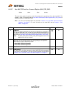
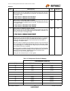
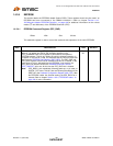
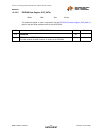
14.2.3.2 General Purpose I/O Data & Direction Register (GPIO_DATA_DIR)
This read/write register configures the direction of the 12 GPIO pins and contains the GPIO input and
output data bits.
Offset: 1E4h Size: 32 bits
BITS DESCRIPTION TYPE DEFAULT
31:28 RESERVED RO -
27:16
GPIO Direction 11-0 (GPIODIR[11:0])
These bits set the input/output direction of the 12 GPIO pins.
0: GPIO pin is configured as an input
1: GPIO pin is configured as an output
R/W 0h
15:12
RESERVED RO -
11:0
GPIO Data 11-0 (GPIOD[11:0])
When a GPIO pin is enabled as an output, the value written to this field is
output on the corresponding GPIO pin. Upon a read, the value returned
depends on the current direction of the pin. If the pin is an input, the data
reflects the current state of the corresponding GPIO pin. If the pin is an
output, the data is the value that was last written into this register. For
GPIOs 11-10 and 7-0, the pin direction is determined by the GPDIR bits of
this register. For GPIOs 9 and 8, the pin direction is determined by the
GPDIR bits and the 1588_GPIO_OE bits in the General Purpose I/O
Configuration Register (GPIO_CFG).
R/W 0h