


Two Port 10/100 Managed Ethernet Switch with 16-Bit Non-PCI CPU Interface
Datasheet
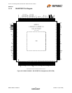
Revision 1.4 (08-19-08) 30 SMSC LAN9311/LAN9311i
DATASHEET
122,125
+3.3V Port 2
Analog Power
Supply
VDD33A2 P +3.3V Port 2 Analog Power Supply
Refer to the LAN9311/LAN9311i application note
for additional connection information.
120
+3.3V Master
Bias Power
Supply
VDD33BIAS P +3.3V Master Bias Power Supply
Refer to the LAN9311/LAN9311i application note
for additional connection information.
121
Port 2
Transmitter
+1.8V Power
Supply
VDD18TX2 P Port 2 Transmitter +1.8V Power Supply: This pin
is supplied from the internal PHY voltage regulator.
This pin must be tied to the VDD18TX1 pin for
proper operation.
Refer to the LAN9311/LAN9311i application note
for additional connection information.
118
Port 1
Transmitter
+1.8V Power
Supply
VDD18TX1 P +1.8V Port 1 Transmitter Power Supply: This pin
must be connected directly to the VDD18TX2 pin
for proper operation.
Refer to the LAN9311/LAN9311i application note
for additional connection information.
Table 3.4 Host Bus Interface Pins
PIN NAME SYMBOL
BUFFER
TYPE DESCRIPTION
25,26,
28-32,
34-38,
41-44
Host Bus
Data
D[15:0] IS/O8 Host Bus Data: Bits 15-0 of the Host Bus data
port.
Note: Big and little endianess is supported.
45,47,
49-53,
55,56
Host Bus
Address
A[9:1] IS Host Bus Address: 9-bit Host Bus Address Port
used to select Internal CSR’s and TX and RX
FIFO’s.
Note: The A0 bit is not used because the
LAN9311/LAN9311i must be accessed on
WORD boundaries.
57
Read Strobe nRD IS Read Strobe: Active low strobe to indicate a read
cycle. This signal is qualified by the nCS chip
select.
58
Write Strobe nWR IS Write Strobe: Active low strobe to indicate a write
cycle. This signal is qualified by the nCS chip
select.
59
Chip Select nCS IS Chip Select: Active low signal used to qualify read
and write operations.
Table 3.3 LAN Port 1 & 2 Power and Common Pins (continued)
PIN NAME SYMBOL
BUFFER
TYPE DESCRIPTION