


ADCP-50-304 • Issue 19 • June 1999 • Section 2: Functional Description
Page 2-13
© 1999, ADC Telecommunications, Inc.
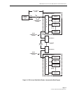
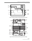
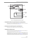
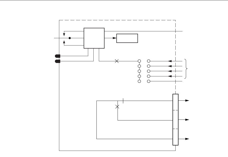
Figure 2-8. A/B Switching Module Simplified Circuit Diagram
5 LED/ALARM PATCH MODULE WITH A/B SWITCHING AND OFF-LINE ACCESS (PSM-04)
This module is the same as PSM-01 except that when it is in the A/B state, the off-line port
provides direct test access to the off-line device (see Figure 2-2).
6 PATCH MODULE WITH A/B SWITCHING AND OFF-LINE ACCESS (PSM-05)
This module is the same as PSM-04 except it does not have LEDs or Alarm.
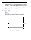
7 LED/ALARM PATCH INTERFACE (PSM-07)
This PS module provides interface patching together with status and alarm indications. A
simplified circuit illustrating patching only is shown in Figure 2-9.
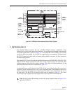
The COMPUTER patch cord jack connects directly to the chassis rear upper interface port. The
MONITOR patch cord jack connects directly to the chassis rear lower interface port. The
monitoring and alarm circuits of the PS module are shown in Figure 2-10. LEDs show the status
of eight RS-232 leads. Each lead has a jumper connection to the alarm circuit control logic. The
A
B
A
B
TOGGLE
SWITCH
A/B
SWITCH
LOGIC
A/B SWITCH CONTROL
A/B
RELAYS
A/B
RELAYS
A/B
INTERLOCK
JUMPER
GROUP 1
2
3
4
V
CONTROL
MODULE
TO CHASSIS
BACKPLANE
1613-A
A/B
RELAY
DTE
(A)
DTE
(B)
DCE
UPPER
INTERFACE
PORT
LOWER
INTERFACE
PORT
VERTICAL
INTERLOCK