


ADCP-50-304 • Issue 19 • June 1999 • Section 7: Operation
Page 7-3
© 1999, ADC Telecommunications, Inc.
The middle port functions in a similar manner for the middle connector on the chassis rear
panel. When in the “B” state, monitor access; “A” state, test access to the off-line “B” device.
The lower port provides intrusive access to the lower connector on the chassis backplane.
Insertion of a patch cord in this port, regardless of switch status, breaks the circuit and connects
the patchcord to the common (DCE) device.
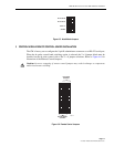
4 INTERFACE MODULE
When an Interface Module is used, it is connected by inserting a patch cord into the MONITOR,
COMPUTER, or MODEM jacks of a PS equipment module. This provides the access to these
jacks to insert test equipment. The computer and modem circuits are split so their operation is
affected. This is not true in the case of the monitor circuit. Test equipment, in this case, is
connected to the chassis rear interface connector(s).
4.1 Test Module
When a test module is used, it is connected in the communications line to access test equipment.
This is first accomplished by inserting a patch cord between either the MONITOR,
COMPUTER, or MODEM patch jacks of a PS equipment module and the test module patch
jack. The test module provides two RS-232/V.24 ports for connecting test equipment on the rear
of the module. Refer to Section 2 for a detailed functional description of the test modules.
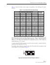
5 SWITCHING
All PS module switching operations are performed in conjunction with the Control Module
(CM). The Control Module is used to enable the switching of all the modules contained in the
PS chassis. Modules in a PS chassis can be switched individually or all at one time (bank
switching). The switches located on the individual modules and Control Module are listed in
Table 7-1.
A bank switching operation switches all of the A/B modules in a PS chassis to either the “A”
position or “B” position. Both individual and banking operations may be done either locally or
remotely.
Caution: The bank switching feature is not compatible with the group interlock feature. If no
module in an interlocked group is in the B state when a bank switch to the B state is initiated,
the first module in this group will switch to the B state. Data may be lost when more than one
module is in the B state. If one module in an interlocked group is in the B state when a bank
switch is initiated, the rest of the modules in that interlock group do not switch to the B state;
consequently, the system maintains its integrity.