


ADCP-50-304 • Issue 19 • June 1999 • Section 3: PatchSwitch V.35
Page 3-5
© 1999, ADC Telecommunications, Inc.
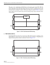
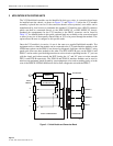
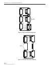
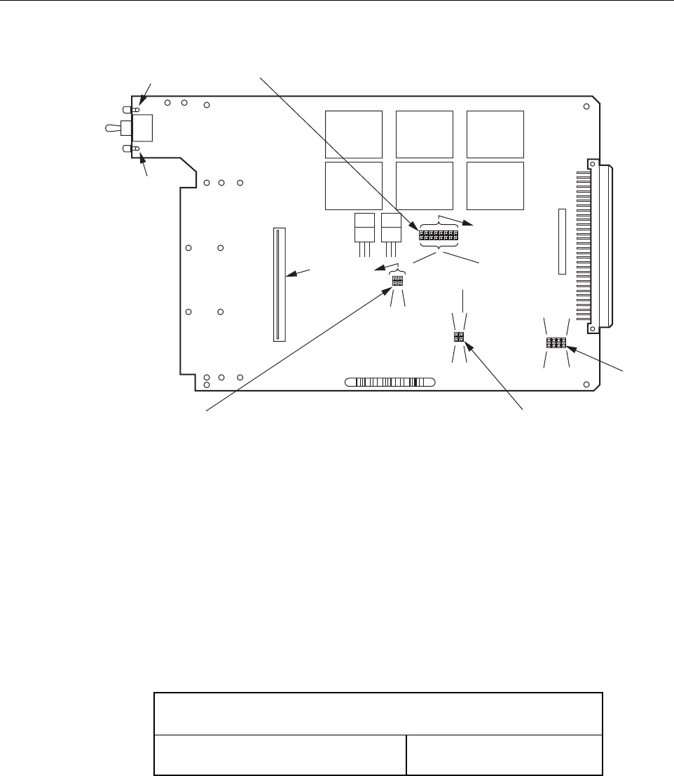
Figure 3-3. PSM-16 and PSM-17 Module PC Board (Component Side)
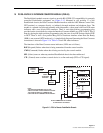
4 FUNCTIONAL SELECTION—CONVERSION BOARD
The item found in Table 3-4 is associated with the conversion board. Refer to Figure 3-4 or
Figure 3-5 for item locations. The option available on the conversion board allows the user the
ability to manage the V.35 lead set. This option, as noted in Table 3-5, allows the user to custom
configure the leads patched in each of his V.35 modules for his specific needs. Normal Pin
Assignments are shown in Table 3-6.
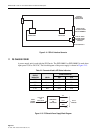
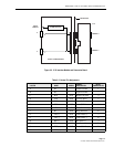
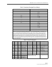
Table 3-4. Optional Item on the Conversion Board
1.
Are any of the normally unassigned leads required by this circuit?
(See Table 3-5)
NO
(Factory Set)
YES
See note on
Table 3-5
TD
RD
RTS
CTS
DCD
TC
RC
DTR
E14
E16
E18
E20
E22
E24
E26
E28
E34
E36
E44
E42
E40
E38
Y
U
AA
W
LCHD
LCHD
ALM +
ALM –
E30
E32
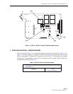
P1
DS1
DS2
1
22
ITEM
B
ITEM
A
ITEM
D
ITEM
C
1625-A