


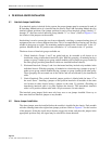

ADCP-50-304 • Issue 19 • June 1999 • Section 6: Installation
Page 6-5
© 1999, ADC Telecommunications, Inc.
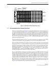
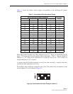
Table 6-1 shows the binary switch settings corresponding to the identifying PS chassis
addresses.
Some older control modules only allow addresses up to “07”. These can be identified by the
digits –7702 at the end of the part number. Models with digits –7708 or –7709 are capable of
addresses to “15”. Both can be intermixed in a system as long as the –7702 versions are
assigned addresses of “07” or below.
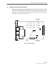
A switch in the ON position represents a zero (0) bit, and conversely, a switch in the down
position (not ON) represents a one (1) bit.
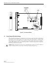
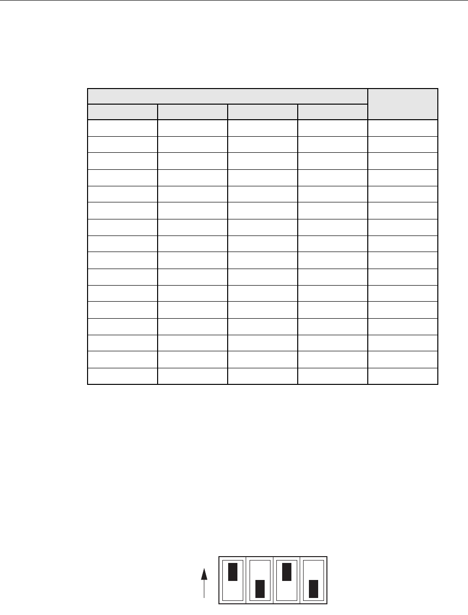
For example, when facing the component side of the CM circuit board, the address for the
chassis number 10 is set as shown in Figure 6-3.
Figure 6-3. Control Module DIP Switch Settings for Chassis 10
Table 6-1. Control Module DIP Switch Address Settings
SWITCH POSITIONS FOR BINARY ADDRESSES
PS CHASSIS
ADDRESS1 2 3 4
On On On On 00
OffOnOnOn01
On Off On On 02
Off Off On On 03
On On Off On 04
Off On Off On 05
On Off Off On 06
Off Off Off On 07
On On On Off 08
Off On On Off 09
On Off On Off 10
Off Off On Off 11
On On Off Off 12
Off On Off Off 13
On Off Off Off 14
Off Off Off Off 15
1636-A
ON
123 4