


ADCP-50-304 • Issue 19 • June 1999 • Section 3: PatchSwitch V.35
Page 3-7
© 1999, ADC Telecommunications, Inc.
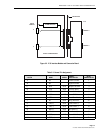
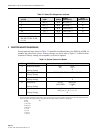
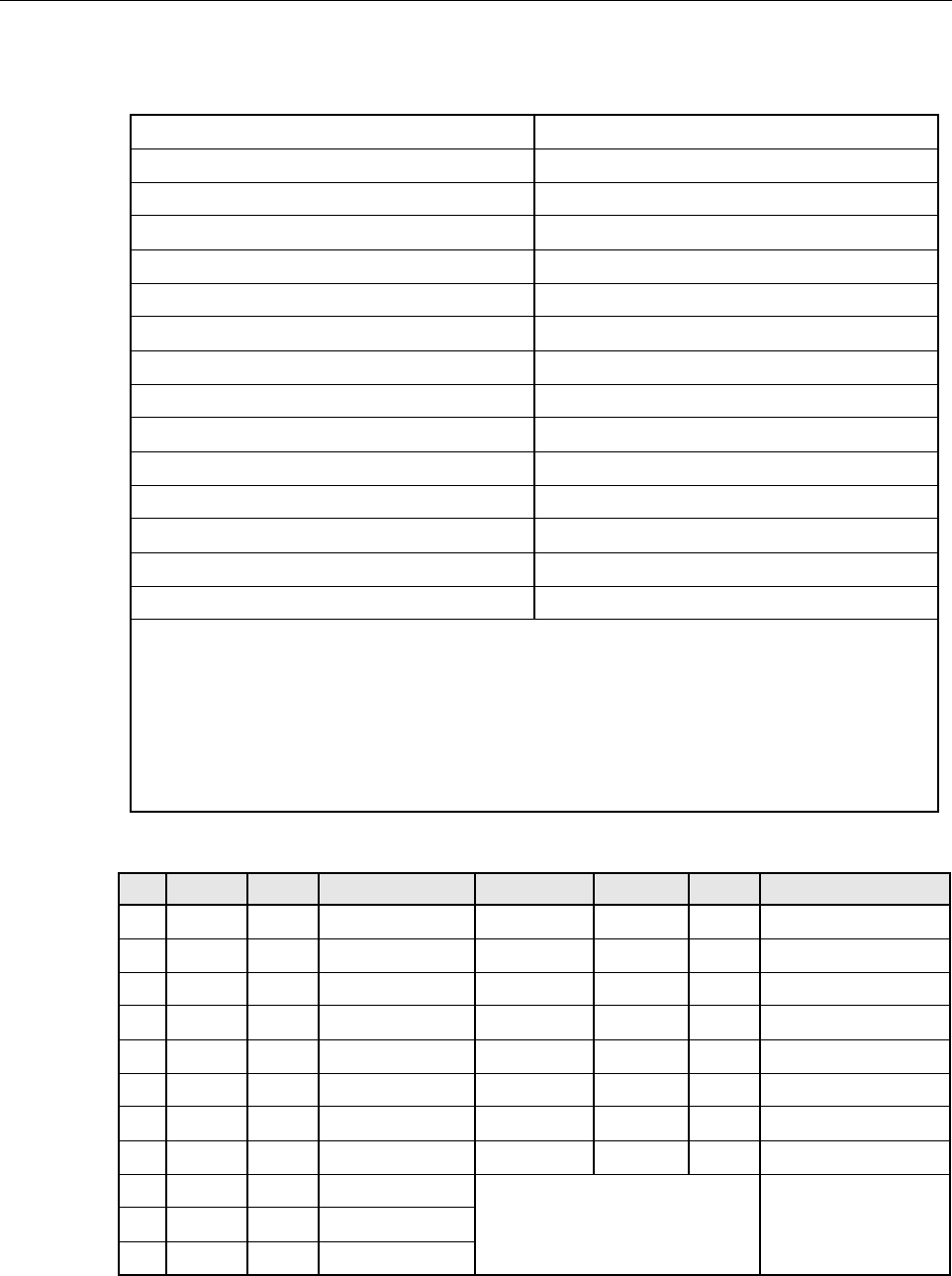
Table 3-5. Connections of Unassigned Pins on Subboard
o---K
o---L
o---M
o---N
oE2 o---Z
oE3 o---BB
oE4 o---CC
oE5 o---DD
oE6 o---EE
oE7 o---FF
o---HH
o---JJ
o---KK
o---LL
o---NN
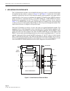
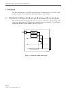
The Pin pattern and identification is as noted above for the fifteen (15) leads unused from the V.35 connector
and the six (6) leads unused through the patching function. Any one of the fifteen leads to a maximum of six
may be routed through the patch mechanism by means of straps if the user desires to bring more than the 19
lead V.35 interface through the patch mechanism. The procedure to follow to add a lead through the patch
mechanism is simple. Assume you desire to bring lead EE through the patch mechanism on a DTE-A, DTE-B,
and DCE module. Simply add a strap from E2 to EE on each of the three connector units on the FFM-01 or
FFM-02 Subboard and lead EE is now routed through the patch mechanism and also switched from A to B if
that action occurs. The procedure for the interface modules is the same. A strap added from E2 to EE on the top
port will cause EE to appear at the top port only. If it is to appear also at the bottom port the additional strap
must also be added there.
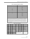
Table 3-6. Normal Pin Assignments
PIN NAME ORIGIN SIGNAL DESCR PIN NAME ORIGIN SIGNAL DESCR
A FG Frame Ground T RD (–) DCE Rec Data (–)
B SG Signal Ground U TCE (+) EXT Trans Clck Ext (+)
C RTS DTE Request to Send W TCE (–) EXT Trans Clck Ext (–)
D CTS DCE Clear to Send X RC (–) DCE Rec Clck (–)
E DSR DCE Data Set Ready V RC (+) DCE Rec Clck (+)
F DCD DCE Data CXR Detect Y TC (+) DCE Trans Clck (+)
H DTR DTE Data Term Ready AA TC (–) DCE Trans Clck (D) (–)
J RI DCE Ring Indicator MM BSY DCE Busy Signal
P TD (+) DTE Trans Data (+) K, L, M, N, Z, BB, CC, DD, EE,
FF, HH, JJ, KK, LL, NN
Unassigned Pins
S TD (–) DTE Trans Data (–)
R RD (+) DCE Rec Data (+)