


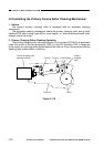
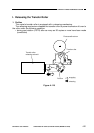

C. Controlling the Development Bias
1. Outline
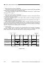
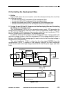
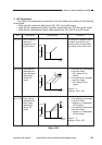
Figure 4-204 shows the circuit used to control the development bias; the circuit has
the following functions:
• turns on and off the AC component of the development bias
• turns on and off the DC component of the development bias
• controls the voltage level of the DC component of the development bias
• controls the DC component of the development bias to a constant level
2. Turning On and Off the DC Component of the Developing Bias and Controlling
the Voltage to a Constant Level
The microprocessor (Q512) on the composite power supply PCB generates the
BPWM signal (pulse signal) under the control of the microprocessor master (Q301) on
the DC controller PCB. In response, the secondary side of the main transformer (T101)
turns on to apply the DC component of the development bias.
In addition, while the DC component of the development bias is being applied, the
application voltage is taken in from the development DC bias voltage detection circuit in
the form of the BIASS signal (analog signal) to exert control so that the output voltage is
maintained at a constant level.
The main transformer (T101) is driven by the drive signal (MPWM) from the
microprocessor (Q512). In addition to the foregoing functions, the main transformer
(T101) is also used as the high-voltage transformer for the DC power supply and other
loads.
Figure 4-204
COPYRIGHT
©
1997 CANON INC. CANON NP6218 REV. 0 MAY 1997 PRINTED IN JAPAN (IMPRIME AU JAPON)
CHAPTER 4 IMAGE FORMATION SYSTEM
4-25
Composite power supply PCB
Main transformer
T101
Transformer (T101)
drive circuit
Development
DC bias drive
circuit
Development
DC bias voltage
detection circuit
Development AC bias
transformer
T301
BPWM
BIASS
MPWM
J211
1~15
J210
1~6
J302
J301
Development
AC transformer
drive circuit
Microprocessor
(Q512)
Photosensitive
drum
Developing cylinder
AE sensor
Copy Density key
DC controller PCB
Microprocessor
(Q301)
Copy density
correction volume
(VR302)
ACBIAS