Central Processing Unit: MPC860P Initialization
PmT1 and PmE1 User’s Manual 10002367-02
3-2
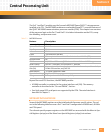
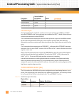
Table 3-2: MPC860P Special Purpose Register Initialization
The internal registers of the MPC860P are mapped to a contiguous 16-kilobyte block of
memory space on a 64-kilobyte boundary. The special purpose register IMMR specifies the
base address of this block. The following table is for the four megabyte PmT1 and PmE1,
some values may change for different configurations.
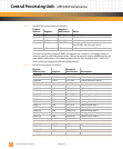
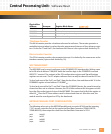
Table 3-3: MPC860P Internal Register Initialization
Decimal
Address: Register:
Required
Hex Format: Notes:
148 ICR 0000,0000 Interrupt cause
149 DER 0000,0000 Debug enable
158 ICTRL 0000,0000 Instruction support control
638 IMMR FF00,0000 Internal memory map sets up the base address of
the MPC860P internal register block
— MSR 1002 Machine State register (control)
Physical
Address (hex): Register:
Required
Hex Format: Description:
General SIU
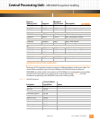
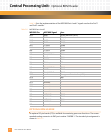
FF00,0000 SIUMCR 7062,3900 SIU module configuration
FF00,0004 SYPCR FFFF,FF08 System protection control
MEMC
FF00,0100 BR0 FFF0,0501 Base register bank 0
FF00,0104 OR0 FFF8,09F4 Option register bank 0
FF00,0108 BR1 0000,0081 Base register bank 1
FF00,010C OR1 FFC0,0000 Option register bank 1
FF00,0110 BR2 0040,0081 Base register bank 2
FF00,0114 OR2 0000,0000 Option register bank 2
FF00,0118 BR3 C100,0001 Base register bank 3
FF00,011C OR3 FFFF,8128 Option register bank 3
FF00,0120 BR4 — Base register bank 4
FF00,0124 OR4 C000,0128 Option register bank 4
FF00,0130 BR6 C000,0401 Base register bank 6
FF00,0134 OR6 FF80,0120 Option register bank 6
FF00,0170 MAMR 4E82,1113 Machine A mode
System Integration Timers
FF00,0200 TBSCR 00C2 Timebase status and control
FF00,0240 PISCR 0082 PIT status and control
Clocks and Reset
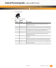
FF00,0280 SCCR 0200,0000 System clock control
Input/Output Por


