Central Processing Unit: Optional BDM Header
10002367-02 PmT1 and PmE1 User’s Manual
3-7
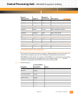
Figure 3-1: Processor BDM Header
Table 3-7: Processor BDM Pin Assignments
Pin
Number:
Signal
Name: Description:
1 VFLSO Visible History Buffer Flushes Status 0 output line reports how
many instructions were flushed from the history buffer in the
MPC860P internal core.
2 SRESET* Software Reset input signal may initiate a warm reset.
3GND1Ground 1
4 TCK Test Clock input scan data is latched at the rising edge of this signal
(1K ohm pull-up to +5 volts, input to board, JTAG bit clock).
5GND2Ground 2
6 VFLS1 Visible History Buffer Flushes Status 1 output line reports how
many instructions were flushed from the history buffer in the
MPC860P internal core.
7 HRESET* Hardware Reset input signal is used at power-up to reset the
processor.
8 TDI Test Data Input signal acts as the input port for scan instructions
and data (1K ohm pull-up to +5 volts, input to board, JTAG data in).
93_3V +3.3 Voltage
10 TDO Test Data Output signal acts as the output port for scan (JTAG)
instructions and data.
1
2
9
10


