


On-Card Memory Configuration: On-card DRAM
10002367-02 PmT1 and PmE1 User’s Manual
4-3
On-card Memory Sizing and Type
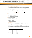
The Board Configuration register (C000,0180
16
) is a byte-wide, read-only register that con-
tains configuration information about the MPC860P and DRAM. Bit (5) is no parity. The con-
figuration registry values are factory set.
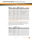
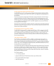
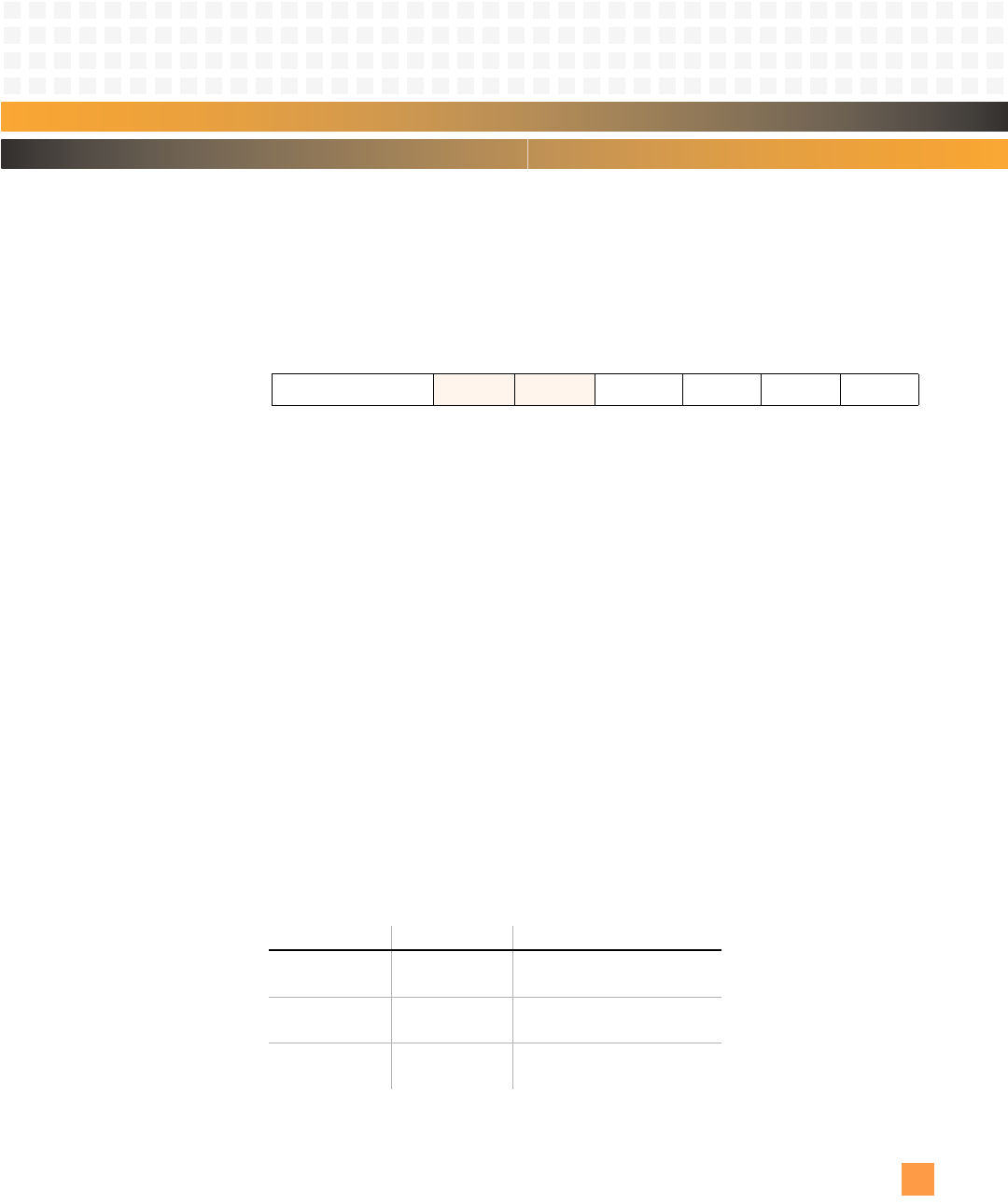
Register 4-1: Board Configuration 0 (BCR), 0x010
LBS: Local Bus Speed
00 Reserved
01 33.33 MHz with 66.66 MHz processor
10 40.00 MHz with 40.00 MHz processor
11 40.00 MHz with 80.00 MHz processor
Bit 4: On-card memory type valued
0 Fast page mode (FPM)
1 Synchronous DRAM (not available)
MEMS/NOB: Memory Size/Number of Banks
0000-0111 Reserved
1000 16/one bank of 16M x 32
DRAM Timing
One of the primary functions of the MPC860P is to allow flexible control of all important
DRAM timing parameters. The correct DRAM timing for any reasonable combination of
board speed and DRAM speed is handled by the user-programmable machine (UPM). The
timing parameters are stored in the UPM’s internal RAM. Reference Chapter 16 in the
MPC860 PowerQUICC™ User’s Manual (Freescale 07/2004, Revision 3) for more details about
the UPM.
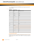
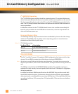
Tab le 4 -3 describes the wait states for the PmT1 and PmE1 module.
Table 4-3: RAM Acess Time
7654 3210
LBS 1 0MEMSNOBMEMSNOB
Cycle: Total Clocks: Wait States:
Reads 4
1
4
2
3
1
3
2
Writes 3
1
3
2
2
1
2
2
Burst Read (4
accesses)
8
1
7
2
3-1-2-1
1
3-1-1-1
2