


Contents
12 Datasheet
Document Number: 278757
Revision Number: 009
Revision Date: 27-Oct-2005
Revision History
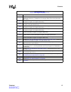
Revision Number: 009
Revision Date: 27-Oct-2005
Page # Description
71 Modified Figure 8 “Ethernet Frame Format” [changed Preamble byte count to 7 bytes].
136 Section 45, “RGMII Power” [changed V
CC
to V
DD in
I
IH
and I
IL
]
110
Added bullet to
Section 5.7.3, “I²C Module Configuration Interface”: The I2C interface only
supports random single-byte reads and does not guarantee coherency when reading two-byte
registers.
227 Replaced Figure 57 “FC-PBGA Package (Top and Bottom Views)” on page 227.
215 Modified Table 147 “SPI3 Receive Configuration ($0x701)”.
222 Modified Table 154 “Optical Module Control Ports 0 - 3 ($0x79A)”: changed default values.
223 Modified Table 155 “I
2
C Control Ports 0 - 3 ($0x79B)”.
249 Modified Table 208 “I2C Data Ports 0 - 9 ($0x79F)” (changed address from $0x79C to $0x79F).
229 Added Section 9.3.3, “Top Label Marking Example”.
230
Modifed Table 157 “Product Information” and Figure 60 “Ordering Information – Sample” under
Section 10.0, “Product Ordering Information”.
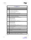
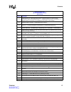
Revision Number: 008
Revision Date: August 1, 2005 (Sheet 1 of 2)
Page # Description
1
Added 552-ball Ceramic Ball Grid Array (CBGA) compliant with RoHS and Product Ordering
Number information.
55
Modified Table 12 “JTAG Interface Signal Descriptions”: changed Standard to 3.3 V LVTTL from
2.5 V CMOS.
72 Modified Figure 9 “PAUSE Frame Format” [changed Preamble byte count to 7 bytes].
85 Modified Figure 11 “MPHY Transmit Logical Timing” [updated TDAT[31:0]].
86 Modified Figure 12 “MPHY Receive Logical Timing” [updated RDAT[31:0]].
88 Modified Figure 14 “SPHY Transmit Logical Timing” [updated TDAT[7:0]].
89 Modified Figure 15 “SPHY Receive Logical Timing” [updated RDAT[7:0] and RPRTY].
121
Modified Figure 31 “Read Timing Diagram - Asynchronous Interface”: changed uPx_ADD[12:0]
to uPx_ADD[10:0].
125 Added paragraphs two and three under Section 5.11, “Loopback Modes”.
129 Changed 3.3 V CMOS to 2.5 V CMOS under Section 5.12.5, “JTAG Clock” on page 129.
131 Added Section 6.2, “Disable and Enable Port Sequences”.
136
Modified Table 45 “RGMII Power” [changed V
OH
, V
OL
, V
IH
, V
IL
minimum conditions to V
DD
and
changed V
IN
value to V
DD
+ .3].
138
Modified Table 46 “SPI3 Receive Interface Signal Parameters” [changed RFCLK duty cycle to
45 min and 55 max; Changed Min for RFCLK frequency to 90].
140
Modified Table 47 “SPI3 Transmit Interface Signal Parameters” [changed TFCLK duty cycle to
45 min and 55 max].
146
Changed MDC to MDIO Output delay max for t3 for 2.5 MHz from 200 to 300 in Table 52 “MDIO
Timing Parameters” on page 146.