


Contents
16 Datasheet
Document Number: 278757
Revision Number: 009
Revision Date: 27-Oct-2005
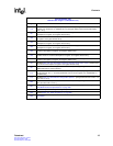
98 Modified Figure 19 “TX_CTL Behavior” [changed signal names].
98 Modified Figure 20 “RX_CTL Behavior” [changed signal names].
99
Modified Section 5.5, “MDIO Control and Interface” [changed 3.3 us to 3.3 ms in fourth paragraph,
third sentence].
103
Modified/replaced all text under Section 5.6, “SerDes Interface” on page 103 [added Table 29
“SerDes Driver TX Power Levels”].
NA Removed old Section 5.6.2.4 AC/DC Coupling.
NA Removed old Section 5.6.2.9 System Jitter.
107
Modified Table 30 “Intel
®
IXF1104 MAC-to-SFP Optical Module Interface Connections” [edited
signal names].
107
Modified/replaced text and deleted old “Figure 19. Typical GBIC Module Functional Diagram” under
Section 5.7, “Optical Module Interface”].
108 Modified second sentence under Section 5.7.2.2.1, “MOD_DEF_0:3”.
109 Modified second sentence under Section 5.7.2.2.3, “RX_LOS_0:3”.
109 Removed third paragraph under Section 5.7.2.2.7, “RX_LOS_INT”.
110 Modified first and second paragraphs under Section 5.7.3, “I²C Module Configuration Interface”.
111 Modified Section 5.7.3.3, “I
2
C Write Operation” [edited portions of text].
116
Modified Table 31 “LED Interface Signal Descriptions” [changed 0.5 MHz to 720 Hz for LED_CLK
under Signal Description].
119
Modified Table 35 “LED Behavior (Fiber Mode)” [changed links under Description to “Link LED
Enable ($0x502)”].
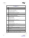
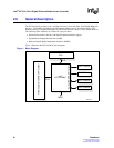
NA Removed old Figure 30 “CPU – External and Internal Connections”.
123 Modified Table 37 “Byte Swapper Behavior” [edited/added new values].
123 Modified second paragraph under Section 5.10, “TAP Interface (JTAG)”
126 Modified Figure 33 “SPI3 Interface Loopback Path”.
126 Added note under Section 5.11.2, “Line Side Interface Loopback”.
127 Modified Figure 34 “Line Side Interface Loopback Path”.
127 Changed Section 5.12, “Clocks” [from GBIC output clock to I
2
C Clock].
129 Changed Section 5.12.6, “I
2
C Clock” [from GBIC Clock to I
2
C Clock].
130 Added new Section 6.0, “Applications”.
132
Modified Table 39 “Absolute Maximum Ratings” [changed SerDes analog power to AVDD1P8_2
and AVDD2P5_2; changed “PLL1_VDDA and PLL2_VDDA to AVDD1P8_1; changed PLL3_VDDA
to AVDD2P5_1.
133
Modified Table 40 “Recommended Operating Conditions” [changed SerDes analog power to
AVDD1P8_2 and AVDD2P5_2; changed “PLL1_VDDA and PLL2_VDDA to AVDD1P8_1; changed
PLL3_VDDA to AVDD2P5_1.
134
Modified Table 42 “SerDes Transmit Characteristics” [included SerDes power driver level
information].
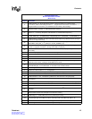
142
Modified Table 49 “GMII 1000BASE-T Transmit Signal Parameters” (changed Min values for t1 and
t2.
143
Modified Table 50 “GMII 1000BASE-T Receive Signal Parameters” (changed Min values for t1 and
t2.
146
Replaced old MDIO Timing diagram and table with Figure 43 “MDIO Write Timing Diagram”, Figure
44 “MDIO Read Timing Diagram”, and Table 52 “MDIO Timing Parameters”.
Revision Number: 007
Revision Date: March 24, 2004
(Sheet 3 of 5)
Page # Description