Contents
18 Datasheet
Document Number: 278757
Revision Number: 009
Revision Date: 27-Oct-2005
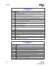
207
Modified Table 136 “Loop RX Data to TX FIFO (Line-Side Loopback) Ports 0 - 3 ($0x61F)”
[renamed heading and bit name].
208
Modified Table 138 “TX FIFO Overflow Frame Drop Counter Ports 0 - 3 ($0x621 – 0x624)”
[renamed from TX FIFO Number of Frames Removed Ports 3 - 0].
209
Modified Table 139 “TX FIFO Errored Frame Drop Counter Ports 0 - 3 ($0x625 – 0x629)” [renamed
from TX FIFO Number of Dropped Packets Ports 0-3 and text under the description].
210 Modified Table 141 “TX FIFO Port Drop Enable ($0x63D)” [changed description for bits 3:0].
211
Modified Table 142 “MDIO Single Command ($0x680)” [changed default; changed description and
default for bits 9:8; changed default for bits 4:0].
212 Modified Table 144 “Autoscan PHY Address Enable ($0x682)” [added note to register description].
213
Modified Table 146 “SPI3 Transmit and Global Configuration ($0x700)” [broke out bits 19:16, 7:4,
and 3:0 and changed description text].
215
Modified Table 147 “SPI3 Receive Configuration ($0x701)” [broke out bits and modified all text
adding SPHY and MPHY modes].
221
Modified Table 152 “Clock and Interface Mode Change Enable Ports 0 - 3 ($0x794)” [deleted
second paragraph of the Register Description; renamed bits to match caption; changed text under
Description].
222 Added note under Section 8.4.11, “Optical Module Register Overview”.
222 Modified Table 153 “Optical Module Status Ports 0-3 ($0x799)” [edited register description].
222 Modified Table 154 “Optical Module Control Ports 0 - 3 ($0x79A)” [changed register description].
NA Removed/Reserved Table 190 “TX and RX AC/DC Coupling Selection ($7x780)”.
NA
Deleted old Figure 19, “Typical GBIC Module Functional Diagram” under Section 5.7, “Optical
Module Interface”.
NA Removed old Section 5.1.1.5, “Pause Command Frames.”
180(old)
Removed old Table 13. TX FIFO Mini Frame Size for MAC and Padding Enable Port 0 to 3 Register
(Addr: 0x63E) and replaced with Reserved.
Revision Number: 006
Revision Date: August 21, 2003
(Sheet 1 of 2)
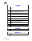
Page # Description
19 Modified Table 1 “Intel
®
IXF1104 Signal Descriptions”
53 Modified Section 5.1.1.1, “Padding of Undersized Frames on Transmit”.
60 Modified text for etherStatsCollision in Table 9 “RMON Additional Statistics”.
87 Modified Table 17 “Intel
®
IXF1104-to-Optical Module Interface Connections”
65 Modified first paragraph under Section 5.3.1.2, “Clock Rates”.
87 Modified Section 5.8.2.1, “High-Speed Serial Interface”.
100 Modified Figure 27 “Microprocessor — External and Internal Connections”.
110 Changed PECL to LVDS under Section 6.1, “DC Specifications”.
113 Modified table note 4 in Table 32 “SPI3 Receive Interface Signal Parameters”.
119 Modified Table 37 “SerDes Timing Parameters”.
125 Modified Table 40 “Microprocessor Interface Write Cycle AC Signal Parameters”.
Revision Number: 007
Revision Date: March 24, 2004
(Sheet 5 of 5)
Page # Description


