


User’s Manual U12978EJ3V0UD
162
CHAPTER 10 REGULATOR
The
µ
PD789800 incorporates a regulator that powers the USB driver/receiver. The features are as follows.
• Generates V
REG
(3.3 ±0.3 V) from V
DD0
, V
DD1
(4.0 to 5.5 V) and outputs it to the REGC pin.
• Supports power-saving mode, reducing power consumption in mode.
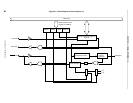
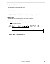
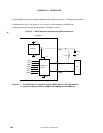
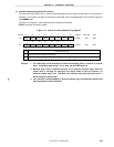
Figure 10-1. Block Diagram of Regulator and USB Driver/Receiver
Regulator
PD789800
RXD
USB driver/
receiver
SEP
SEM
TXDP
TXDM
TXEN
RXEN
V
DD0
VSS0
VSS
VREG
VDD0
VSS0
USBDM
Hub
REGC
22 F
1.5 kΩ
USBDP
µ
µ
Cautions 1. To stabilize the VREG voltage, connect the REGC pin to VSS via 22
µ
µµ
µ
F capacitor.
2. Connect the pull-up resistor (1.5 kΩ
ΩΩ
Ω) for the USBDM pin to the REGC pin.