


CHAPTER 16 ELECTRICAL SPECIFICATIONS
User’s Manual U12978EJ3V0UD
212
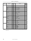
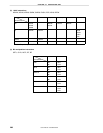
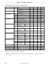
DC Characteristics (TA = −
−−
−40 to +85°
°°
°C, VDD = 4.0 to 5.5 V) (1/2)
Parameter Symbol Conditions MIN. TYP. MAX. Unit
Per pin −1mAOutput current, high I
OH
Total for all pins −15 mA
Per pin 10 mAOutput current, low I
OL
Total for all pins 80 mA
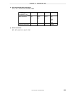
V
IH1
P00 to P07, P10 to P17 0.7V
DD
V
DD
V
V
IH2
RESET, P20 to P26, P40 to P47 0.8V
DD
V
DD
V
V
IH3
X1 V
DD
− 0.1 V
DD
V
Input voltage, high
V
IH4
USBDM, USBDP T
A
= 0 to +70°C2.0 3.6V
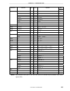
V
IL1
P00 to P07, P10 to P17 0 0.3V
DD
V
V
IL2
RESET, P20, P22, P40 to P47 0 0.2V
DD
V
V
IL3
X1 0 0.1 V
Input voltage, low
V
IL4
USBDM, USBDP T
A
= 0 to +70°C0 0.8V
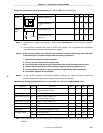
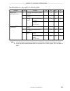
V
OH1
Pins other than USBDM
and USBDP
I
O
= −1 mA V
DD
− 1.0 VOutput voltage, high
V
OH2
USBDM, USBDP T
A
= 0 to +70°C,
RL = 15 kΩ (connected to V
SS
)
Note
2.8 V
V
OL1
Pins other than USBDM
and USBDP
I
O
= 10 mA 1.0 VOutput voltage, low
V
OL2
USBDM, USBDP T
A
= 0 to +70°C,
RL = 15 kΩ (connected to V
DD
)
Note
0.3 V
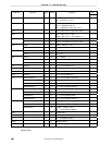
I
LIH1
Pins other than X1, X2,
USBDM, and USBDP
V
I
= V
DD
3
µ
A
I
LIH2
X1, X2 V
I
= V
DD
20
µ
A
Input leakage current, high
I
LIH3
USBDM, USBDP
T
A
= 0 to +70°C
0 V ≤ V
I
≤ V
REG
10
µ
A
I
LIL1
Pins other than X1, X2,
USBDM, and USBDP
V
I
= 0 V −3
µ
A
I
LIL2
X1, X2 V
I
= 0 V −20
µ
A
Input leakage current, low
I
LIL3
USBDM, USBDP
T
A
= 0 to +70°C
0 V ≤ V
I
≤ V
REG
−10
µ
A
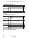
Output leakage current, high I
LOH
V
O
= 0 V 3
µ
A
Output leakage current, low I
LOL
V
O
= 0 V −3
µ
A
Software pull-up resistance R V
I
= 0 V 50 100 200 kΩ
Regulator output voltage V
REG
I
O
= 0 to −3 mA 3.0 3.3 3.6 V
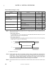
Note RL is the resistance connected to the bus line.
Remark Unless specified otherwise, the characteristics of alternate-function pins are the same as those of port
pins.