


CHAPTER 4 PORT FUNCTIONS
User’s Manual U12978EJ3V0UD
70
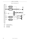
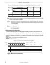
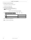
Table 4-3. Port Mode Register and Output Latch Settings When Using Alternate Functions
Secondary Function
Name Input/Output
P26 TO01 Output 0 0
TI01 Input 1 ×
INTP0 Input 1 ×
P40 to
P47
Note
KR00 to KR07 Input 1 ×
Note Set key return mode register 00 (KRM00) to 1 when using the alternate function (see Section 11.3 (5)
Key return mode register 00 (KRM00)).
Caution When Port 2 is used as a serial interface pin, the I/O latch or output latch must be set
according to its function. For the setting method, see Table 9-2 Settings of Serial interface
10 Operating Mode.
Remark x: Don’t care
PMxx: Port mode register
Pxx: Port output latch
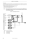
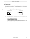
(2) Pull-up resistor option register 0 (PU0)
The pull-up resistor option register (PU0) sets whether an on-chip pull-up resistor on each port is used or not.
On the port which is specified to use the on-chip pull-up resistor in the PU0, the pull-up resistor can be internally
used only for the bits set to the input mode. No on-chip pull-up resistors can be used for the bits set in the
output mode regardless of the setting PU0. This applies to the case when using the output pins for alternate
functions.
PU0 is set with a 1-bit or 8-bit memory manipulation instruction.
RESET input sets PU0 to 00H.
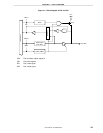
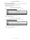
Figure 4-12. Format of Pull-up Resistor Option Register 0
Caution Bits 3 and 5 to 7 must be set to 0.
PxxPMxxPin Name
Pm on-chip pull-up resistor selection
(m = 0 to 2, 4)
0 0 0 PU04 0 PU01 PU00PU0
Address After reset R/W
FFF7H 00H R/W
7 6 5 <4> 3 <2> <1> <0>
PU0m
0
1
On-chip pull-up resistor not connected
On-chip pull-up resistor connected
Symbol
PU02