


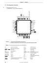
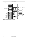

CHAPTER 2 PIN FUNCTIONS
User’s Manual U12978EJ3V0UD
29
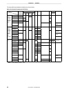
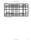
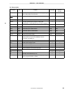
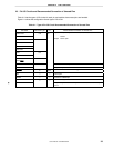
(2) Non-port pins
Pin Name I/O Function After Reset Alternate
Function
INTP0 Input External interrupt request input for which valid edge (rising
and/or falling edge) can be specified
Input P26/TI01/TO01
KR00 to
KR07
Input Input for detecting key return signals Input P40 to P47
NC — No connection. Can be left open. — —
REGC — Internally generated power supply for driving USB
driver/receiver. Connect this pin to V
SS
via a 22
µ
F capacitor.
——
RESET
Input System reset input Input —
SCK10
I/O Serial clock input/output for serial interface Input P20
SI10 Input Serial data input for serial interface Input P22
SO10 Output Serial data output for serial interface Input P21
TI01 Input External count clock input to 8-bit timer TM01 Input P26/INTP0/TO01
TO01 Output Output from 8-bit timer TM01 Input P26/INTP0/TI01
USBDM I/O Serial data input/output (negative side) for USB function. The
pull-up resistor (1.5 kΩ) for the USBDM pin must be
connected to the REGC pin.
Input —
USBDP I/O Serial data input/output (positive side) for USB function Input —
V
DD0
— Positive power supply for ports — —
V
DD1
— Positive power supply for circuits other than ports — —
V
SS0
— Ground potential for ports — —
V
SS1
— Ground potential for circuits other than ports — —
X1 Input Input —
X2 —
Crystal resonator connection to for system clock oscillator
——
IC — Internally connected directly to V
SS0
——
V
PP
— Sets flash memory programming mode. Apply high voltage
when a program is written or verified.
——