


Table of Contents|ASDA-B Series
Revision February 2008, Doc. Name: 2006PDD23000009
3.2 Basic Wiring................................................................................................................................. 3-9
3.3 Input / Output Interface Connector -CN1..................................................................................... 3-12
3.3.1 CN1 Terminal Identification .............................................................................................. 3-12
3.3.2 Signals Explanation of Connector CN1............................................................................ 3-13
3.3.3 User-defined DI and DO signals....................................................................................... 3-18
3.3.4 Wiring Diagrams of I/O Signals (CN1).............................................................................. 3-20
3.4 Encoder Connector CN2 ............................................................................................................. 3-24
3.5 Serial Communication Connector CN3 ....................................................................................... 3-25
3.5.1 CN3 Terminal Layout and Identification ........................................................................... 3-25
3.5.2 Connection between PC/Keypad and Connector CN3 .................................................... 3-26
3.6 Standard Connection Example.................................................................................................... 3-27
3.6.1 Position Control Mode ...................................................................................................... 3-27
3.6.2 Speed Control Mode......................................................................................................... 3-28
3.6.3 Torque Control Mode........................................................................................................ 3-29
Chapter 4 Display and Operation........................................................................................... 4-1
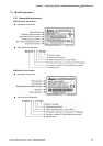
4.1 ASD-PU-01A ............................................................................................................................... 4-1
4.1.1 Description of Digital Keypad ASD-PU-01A..................................................................... 4-1
4.1.2 Display Flowchart ............................................................................................................. 4-3
4.1.3 Status Display................................................................................................................... 4-8
4.1.4 Fault Code Display Operation .......................................................................................... 4-11
4.1.5 JOG Operation.................................................................................................................. 4-12
4.1.6 DO Force Output Diagnosis Operation ............................................................................ 4-14
4.1.7 DI Diagnosis Operation .................................................................................................... 4-15
4.1.8 DO Diagnosis Operation................................................................................................... 4-15
4.1.9 Parameters Read and Write............................................................................................. 4-16