Management Processor CPLD: MPC8548 PLD Register
ATCA-9305 User’s Manual 10009109-01
5-12
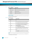
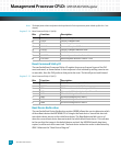
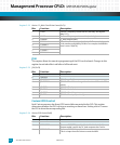
Register 5-22: Cavium 2 C_MULL Clock Divisor Control (0x74)
JTAG
This register allows for manual reprogramming of the PLDs on the board. Changes to this
register do not take effect until after a full board reset.
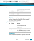
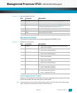
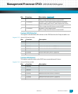
Register 5-23: JTAG (0x78)
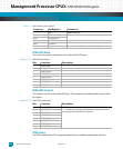
Cavium GPIO Control
Each Cavium processor has three GPIO control bits connected to the PLD. This register
determines whether the PLD is driving or receiving on these lines. Setting a bit to 1 causes
the PLD to drive the corresponding line.
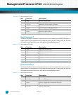
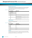
Register 5-24: Cavium GPIO Control (0x80)
Bits: Function: Description:
7 CAVF1 Cavium 1 Frequency resistor set bit (read-only, see Register
Map 5-21)
6 CAVF0 Cavium 0 Frequency resistor set bit (read-only)
5CMULOE C_MUL Output Enable
4 P1CMUL4 These bits drive directly to the Cavium 2. The core clock speed
is the number multiplied by 50 MHz. For example, the 800 MHz
core is set to 16(0x10).
3P1CMUL3
2P1CMUL2
1P1CMUL1
0P1CMUL0
Bits: Function: Description:
7 reserved
6 reserved
5 JTAGOEN JTAG Output Enable
4 JTAGTCKSEL JTAG Test Clock Select changes from header to PLD as the TCK
source
3JTAGTCK JTAG Test Clock
2 JTAGTMS JTAG Test Mode Select
1JTAGTDO JTAG Test Data Output
0 JTAGTDI JTAG Test Data Input (read only)
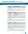
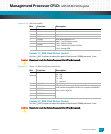
Bits: Function: Description:
7 reserved
6 reserved
5 P2GPIO5OE Processor 2 GPIO5 Output Enable (enabled is the default)
Output enable is set for the TIC timer output to the Cavium
4 P2GPIO4OE Processor 2 GPIO4 Output Enable
This is an input from the Cavium to reset the MIP4


