


Model 5328A
List of Figures
LIST OF FIGURES
4-1.
4-2.
4-3.
4-4.
4-5.
4-6.
4-7.
4-8.
4-9.
4-10.
5-1.
5-2.
5-3.
5-4.
5-5.
5-6.
5-7.
5-8.
5-8.
5-9.
5-10.
5-10.
5-10.
5-11.
5-11.
5-12.
8-1.
8-2.
8-3.
8-4.
8-5.
8-6.
8-7.
8-7.
8-8.
8-9.
8-10.
8-11.
8-12.
8-13.
8-14.
8-15.
8-16.
8-17.
8-18.
8-19.
8-20.
8-21.
8-22.
8-23.
8-24.
8-25.
Basic Elements of the Frequency Counter
. . . . . . . . . . . . . . . . . . . . . . . . . . .
Measuring Period . .
. . . . . . . . . . . . . . . . . . . . . . . . . . . . . . . . . . . . . . . . . . . . . . .
Basic Elements of a Time interval Counter . . . . . . . . . . . . . . . . . . . . . . . . . .
Clock Pulses
. . . . . . . . . . . . . . . . . . . . . . . . . . . . . . . . . . . . . . . . . . . . . . . . . . . . .
Synchronizer Operation with Time Interval Averaging
. . . . . . . . . . . . . . .
±1 Count Ambiguity
. . . . . . . . . . . . . . . . . . . . . . . . . . . . . . . . . . . . . . . . . . . . . .
Trigger Error
. . . . . . . . . . . . . . . . . . . . . . . . . . . . . . . . . . . . . . . . . . . . . . . . . . . . .
Block Diagram . . . . . . . . . . . . . . . . . . . . . . . . . . . . . . . . . . . . . . . . . . . . . . . . . . .
Remote Controllable (Programmable) Input Block Diagram
. . . . . . . . .
ASM Oscillator Timing Diagram . .
. . . . . . . . . . . . . . . . . . . . . . . . . . . . . . . . .
10 MHz Oscillator Frequency Check
. . . . . . . . . . . . . . . . . . . . . . . . . . . . . .
DAC Adjustment Equipment Connectors
. . . . . . . . . . . . . . . . . . . . . . . . . .
DAC Adjustment Oscilloscope Readout and Adjustment Locations . .
Hookup for A3 Oscillator Support Adjustment
. . . . . . . . . . . . . . . . . . . . .
A3 Jitter Adjustment . . . .
. . . . . . . . . . . . . . . . . . . . . . . . . . . . . . . . . . . . . . . . .
System Configuration
. . . . . . . . . . . . . . . . . . . . . . . . . . . . . . . . . . . . . . . . . . . .
Sample Printout
. . . . . . . . . . . . . . . . . . . . . . . . . . . . . . . . . . . . . . . . . . . . . . . . .
Hookup for
Hookup for Test Described in Table 5-8B and C . . . . . . . . . . . . . . . . . . . .
Triangular Pulse Observed in Steps 5 and 7, Table 5-8B
. . . . . . . . . . . . .
Assembly Flowchart (Sheet 1 of 3) . .
. . . . . . . . . . . . . . . . . . . . . . . . . . . . . . .
Assembly Flowchart (Sheet 2 of 3)
. . . . . . . . . . . . . . . . . . . . . . . . . . . . . . . . .
Assembly Flowchart (Sheet 3 of 3) . .
. . . . . . . . . . . . . . . . . . . . . . . . . . . . . . .
Local Troubleshooting Flowchart (Sheet 1 of 2) . . . . . . . . . . . . . . . . . . . . .
Local Troubleshooting Flowchart (Sheet 2 of 2) . . . . . . . . . . . . . . . . . . . . .
Address Switch Troubleshooting Flowchart
. . . . . . . . . . . . . . . . . . . . . . . .
Schematic Diagram Notes . .
. . . . . . . . . . . . . . . . . . . . . . . . . . . . . . . . . . . . . . .
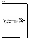
5328A Front View
. . . . . . . . . . . . . . . . . . . . . . . . . . . . . . . . . . . . . . . . . . . . . . . . .
5328A Rear View
. . . . . . . . . . . . . . . . . . . . . . . . . . . . . . . . . . . . . . . . . . . . . . . . .
5328A Top View
. . . . . . . . . . . . . . . . . . . . . . . . . . . . . . . . . . . . . . . . . . . . . . . . . .
5328A Bottom View
. . . . . . . . . . . . . . . . . . . . . . . . . . . . . . . . . . . . . . . . . . . . . . .
A1 Motherboard . . . . . . . . . . . . . . . . . . . . . . . . . . . . . . . . . . . . . . . . . . . . . . . .
A1 Motherboard Schematic and Components (Sheet 1 of 2) . . . . . . . . .
A1 Motherboard Schematic and Components (Sheet 2 of 2)
. . . . . . . . .
A2 Power Supply Block Diagram . .
. . . . . . . . . . . . . . . . . . . . . . . . . . . . . . . .
A2 Power Supply Schematic and Components . . . . . . . . . . . . . . . . . . . . . .
4-1
4-2
4-3
4-3
4-5
4-5
4-7
4-8
4-14
4-24
5-19
5-22
5-23
5-24
5-25
5-31
5-32
5-36
5-38
5-47
5-49
5-51
5-52
5-53
5-54
8-3
8-7
8-7
8-8
8-9
8-11
8-17
8-19
8-18
8-19
A3/A3A1 Oscillator Support Schematic and Components . . . . . . . . . . . . . 8-21
A4 Function Selector Block Diagram
. . . . . . . . . . . . . . . . . . . . . . . . . . . . . .
8-23
A4 Function Selector Schematic and Components . . . . . . . . . . . . . . . . . .
8-25
A8 Channel “C” Block Diagram . . . . . . .
. . . . . . . . . . . . . . . . . . . . . . . . . . . .
8-26
A8 Channel “C” Schematic and Components
. . . . . . . . . . . . . . . . . . . . . .
8-27
A10 Synchronizer Block Diagram
. . . . . . . . . . . . . . . . . . . . . . . . . . . . . . . . . .
8-28
A10 Synchronizer Schematic and Components
. . . . . . . . . . . . . . . . . . . . .
8-29
A11 Digital-to-Analog Converter Block Diagram . . . . . . . . . . . . . . . . . . . .
8-30
A11 Digital-to-Analog Converter Schematic and Components
. . . . . . .
8-31
A12 “A-B” Channel Block Diagram
. . . . . . . . . . . . . . . . . . . . . . . . . . . . . . . .
8-32
A12 “A-B” Channel Schematic and Components . . . . . . . . . . . . . . . . . . .
8-33
A15 HP-IB Interface Block Diagram
. . . . . . . . . . . . . . . . . . . . . . . . . . . . . .
8-35
A15 HP-IB Interface Schematic and Components
. . . . . . . . . . . . . . . . . . .
8-37
A16 Display Block Diagram . . . . . . . . . . .
. . . . . . . . . . . . . . . . . . . . . . . . . . . .
8-39
A16 Display Schematic and Components
. . . . . . . . . . . . . . . . . . . . . . . . . .
8-41
A19 Switch/Attenuator Schematic and Components
. . . . . . . . . . . . . . . .
8-43
vii