


Model 5328A
Theory of Operation
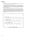
4-155. Averager U4 converts the current pulses supplied via CR10 into a dc output voltage.
The averager generates the output voltage proportional to the duty cycle of the input current
pulses.
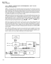
4-156. A8 Channel C Input
4-157, The A8 board contains circuitry to amplify and detect input signals up to 500 MHz, a
divide-by-10 counting chain, a high-speed gate, and circuitry to drive the least-significant-
digit in the display.
4-158, The input signal enters J1 and continues through a fuse (F1) into a limiter circuit com-
posed of diodes CR2-5 and a 50-ohm termination. Diodes CR2-5 have 70V reverse breakdown
voltage and limit the signals below that value to approximately ±600 mV to protect amplifier
U1. Fuse (F1) is rated at 125 mA and blows when the input voltage reaches about =7 volts. The
signal passes through amplifier U1 (with a single ended gain of =4) and drives U2 (a combination
amplifier/Schmitt trigger) differentially. The Schmitt trigger output (U2 pin 13) is a logic level
from 0 volts to approximately -600 mV. The now digital (square wave) signal passes through
U3 where it branches to drive a binary (U4) and a detector. The detector circuit senses the
presence of an input signal and sends a TTL “C ARM” command to the A4 Function Selector,
as described in the following paragraph.
4-159. During normal operation (in the frequency C function) U4 is originally disabled by a
High logic level at U4 pin 14 (0 volts). When the counter is ready to make a measurement and
it senses that an input signal is present via the “C ARM” line, the main gate opens. Pin 14 on
U4 then goes “low” (to -600 mV) and the input signal passes through U4
(+5)
where it is trans-
lated to ECL levels. A 50-40% duty cycle (for sine wave inputs) signal is sent to the A4 Function
Selector on “C” and
“~”
bus lines, after the time base counts out, the main gate closes, U4 pin
14 goes high and U4 and U5 stop in their present states. Circuit U6 translates the information in
U4–U5 to TTL level and it is shifted into a quad latch (U7) where it is stored for strobing into
the display.
4-160. Circuit U10, Q1, Q2, and various resistors constitute a current source to properly bias
U1 and U2. The circuit draws approximately 16 mA out of pin 3 on each IC and adjusts the cur-
rent out of pin 6 between 28 and 56 mA until the voltage on pin 3 is approximately +600 to
+900 mV on each IC.
4-161. Resistors R1, R2, R4, and R82 and U9A comprise the offset voltage adjustment circuit.
This circuit also compensates for changes in input bias current into U1 to minimize drift in
offset voltage.
4-162. HP INTERFACE BUS THEORY
4-163. The HP Interface Bus transfers data and commands between the components of an
instrumentation system on 16 signal lines. The interface functions for each system component
are performed within the component so only passive cabling is needed to connect the system.
The cables connect all instruments, controllers, and other components of the system in parallel
to the signal lines.
4-164. Eight of the lines (DIO1—DIO8) are reserved for the transfer of data and other messages
in a byte-serial, bit-parallel manner. Data and message transfer is asynchronous, coordinated
by the three handshake lines (DAV, NRFD, NDAC). The other five lines are for control of bus
activity,
4-165. Devices connected to the bus may be talkers, listeners, or controllers. The controller
dictates the role of each of the other devices by setting the ATN (attention) line low and sending
4-20