


Model 5328A
Theory of Operation
Since the condition of the MA and MB lines remains the same, the Channel A DAC receives
the clock pulses. On the negative transition of the clock pulse, the + or - is shifted into the A
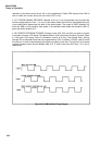
channel DAC shift registers A10U7 and U11.
4-145. Following the format, the next data byte on MDA-MDD will be a number. The MDA-
MDD lines supplied to U7 are also connected to the A11 DAC board shift registers. Since the
interface is in the DAC mode, neither U8 or U15 are clocked and thus disregard data on MDA-
MDD. The number is clocked into the A channel DAC shift registers. The condition of the MA
and MB lines, determines which DAC is clocked and accepts the number. Following the first
number, a decimal appears at the input to ROM U7. When U7 decodes the decimal, it sends
U7(5) high. This high, applied to U2(15), causes U2 to block the clock pulse associated with the
decimal data byte.
In this manner, the DAC disregards the decimal.
4-146. Following the format, two more numbers are input, serially, and each clocked into the
A channel DAC shift registers. The final character in the string, an asterisk (*), appears on the
input data lines to U7. When U7 decodes the asterisk, U7(5) goes high, again blocking the
positive clock pulse transition to the A channel DAC. This causes the A channel DAC to disre-
gard the *. Simultaneously U7(6) goes low, allowing the negative transition of the clock pulse
to latch the low at U8(13) into U8(12). The low at U8(12) causes U17(8) to go low, returning the
interface to the non-DAC control mode.
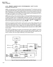
4-147. A11 DAC Board
4-148. Since the DAC board contains two identical DACs only the Channel A DAC will be
discussed. For the following description assume the Channel A DAC is programmed for a
+2.22V trigger level. Refer to Program Code Set, Table 3-5, for an explanation of the format.
4-149. The first data byte, a +, appears on the input data lines MDA-MDD. This data byte is
supplied to the inputs of shift registers U7 and U11. An LMS clock pulse routed through A10U6,
applied to U7 pin 1, shifts the + into U7 and U11. The next three data bytes, all two’s, are shifted
into U7 and U11 in the same manner.
4-150. With the + and the three numerals shifted into U7 and U11, the shift registers provide
a parallel BCD output. This parallel output is static until the A channel DAC is reprogrammed.
The parallel output is supplied to the input of rate multiplier chain U8, U9, and U10.
4-151. Circuit USC and related components are configured as an oscillator. The oscillator
output is coupled through Q7 to the clock input of rate multipliers U8, U9, and U10. The clock
signal is also supplied through inverter U5D to D-FF U2A, which is used as a synchronizer and
wave shaper.
4-152. With 1000 pulses entering pin 9 of each rate multiplier, the output at U10(6) will be
222 pulses, These pulses are supplied through level shifter and inverter U5B to U2(12), The in-
put pulese are synchronized and shaped by U2A, The Q and Q outputs, from U2A, supply level
shifter networks composed of resistors R31, R34, and R36, R38, and R39. The pulse outputs
from the level shifter networks arrive at the cathode of CR6 and the anode of CR8.
4-153. The + shifted into U11, causes U6 pins 2 and 6 to go high, The highs, on pins 2 and 6,
cause pins 1 and 7 to go low. The low at U6(1), causes CR11 to be forward biased. Forward bias-
ing CR11 causes U6A to sink all of the current from the positive current source, This disables
the positive current source U3A and Q3. With U6(7) low, CR12 is reverse biased enabling the
negative current source U3B and Q4.
4-154. The signal at the anode of CR8 is the inverted output from the rate multipliers. When
the anode of CR8 is low, CR8 is reverse biased, and current flows through CR10 into U4(2), When
the anode of CR8 is high, CR8 is forward biased and current flows from Q4 through CR8
4-19