


Model 5328A
Maintenance
c.
d.
e.
f.
g.
h.
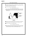
Set 5328A rear panel control as follows:
ARM . . . . . . . . . .
. . . . . . . . . . . . . . . . . . . . . . . . . . . . . . . . . . . . .
OFF
Connect HP 608E Signal Generator (or equivalent) to INPUT A. Set signal gen-
erator to 35 MHz at 50 mV rms (140 mV p-p).
Slowly decrease the signal generators output level to 15 mV rms (42 mV p-p),
while adjusting variable resistor R26, to obtain a stable correct display, on the
counter.
To set Channel B sensitivity change 5328A front panel controls as follows:
FUNCTION . . . .
. . . . . . . . . . . . . . . . . . . . . . . . . . . . . .
RATIO B/A
RESOLUTION . .
. . . . . . . . . . . . . . . . . . . . . . . . . . . . . . .
1(33
10 kHz
SEP-COM A
. . . . . . . . . . . . . . . . . . . . . . . . . . . . . . . . . . . . . . . . . .
SEP
LEVEL B
. . . . . . . . . . . . . . . . . . . . . . . . . . . . . . . . . . . . . . . . . . .
PRESET
With HP 651B Test Oscillator (set to 10 MHz at 100 mV rms) connected to lN-
PUT A, connect a second signal generator (set to 40 MHz at 50 mV rms) to iN-
PUT B.
Repeat step e adjusting variable resistor R28 instead of R26.
2.
Channel C Sensitivity adjustments:
a.
Remove the top cover from the 5328A.
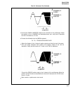
b. Set signal to 100 MHz and reduce level until no stable reading in counter dis-
play. Adjust A8R82 for stable reading.
c.
Repeat step b. until best sensitivity is obtained.
d. Repeat step b. to ensure that the counter still meets the requirement.
3.
High Frequency Offset adjustments:
a.
Remove top cover.
b. Set signal generator to 500 MHz and reduce signal level until display reading
is no longer stable. Adjust A8R85 until display is stable.
c.
Repeat step b. until best balance is obtained.
4.
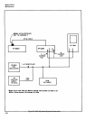
D-to-A Converter Adjustment procedure:
The following adjustment procedure adjusts the All D-to-A Converter outputs for accurate
programmed trigger levels. Measuring the DAC outputs with a DVM is NOT an equivalent
procedure. Since the gain through the 5328A input amplifiers is not exactly equal to 1.00,
the signal arriving at the A12U4 comparator is not identical to the signal at the counter’s
input. As an example, assume the input amplifier gain is 0.95. Further assume an input signal
which goes from 0 volts to 1.0 volt and it is desired to trigger at the 1.0 volt level. Since the
signal arriving at A12U4 goes from 0 volts to 0.95 volts (due to the gain of 0.95), the trigger
level specified by the DAC to A12U4 must be 0.95 volts. Triggering at 0.95 volts on the A12U4
input signal is the same as triggering at the 1.0 volt level on the original signal. The procedure
described in the following takes into account the fact that the input amplifier gain is less
than 1.0.
The procedure offsets an input signal to the 5328A by 0, +2, and -2 volts and programs the
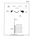
A and B channel trigger levels for 0, +2, and -2 volts respectively. For each offset, adjustments
are made by observing the A (and B) channel marker outputs and adjusting for a 50% duty
cycle. A 50% duty cycle indicates that the programmed trigger level (which is the center of
the hysteresis band) is exactly equal to the dc offset at the signal input to the A12U4
comparator.
5-20