


Model 5328A
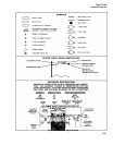
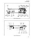
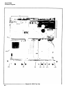
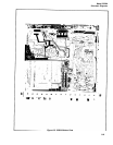
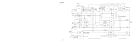
Schematic Diagrams
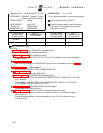
Table 8-1. Signal Mnemonics (Continued)
MNEMONIC
DESCRIPTION
OSC
100 MHz oscillator. ECL levels.
OSC
OVFL
Overflow. TTL active low indicates display overflow.
RG
ROM bit. Used to recognize period and institute hysteresis
compensation. TTL level.
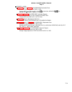
RL1 (HEC)
Latched ROM bit. TTL level enables channel C to strobe its
digit onto the bus.
RL2 (BIL)
Latched ROM bit. High for time interval average. TTL level.
RL3 (HDVM)
Latched ROM bit. Enables DVM to strobe a minus sign on
the display or blank characters. TTL level.
RL4 (LTIF)
Latched ROM bit. TTL level low in time interval or period
measurement.
RL5 (TIO)
Latched ROM bit. TTL level used to recognize period
average.
RL6 (HC)
Latched ROM bit which turns hysteresis compensation on
and has a time interval as opposed to a period measurement
made by the Time Interval unit, TTL level.
SRT
The charge node line that controls the sample rate speed.
RL (TBA)
RL (TBB)
Latched ROM bits that drive Time Base select code inputs.
RL (TBC)
TBI
TTL signal that drives Time Base.
TBO
Time Base scaled output. TTL levels.
TBS Code A (TBSA)
Time Base code input to ROM controlled by the Time
TBS Code B (TBSB)
Base switch. TTL levels.
TBS Code C (TBSC)
TI
Time interval. Output of Time Interval module used in
TI time interval measurements, ECL levels.
8-6