


Model 5328A
Theory of Operation
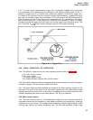
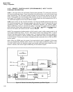
4-77. All measurements performed by the 5328A result in pulses being counted in the DCA.
Pulses are admitted to the DCA by way of the Main Gate FF on A4 which is either controlled
by a Gate Out signal from the Time Base (A1U19) or held open by the HOPN signal from A1U25.
4-78. Data strobe signals, transfer pulses, reset pulses, and an output disabling signal are
routed to the DCA via the 5328A State Control Circuitry. These signals are processed in the
DCA and are used to control transfer of the counter’s output data to the latch outputs, strobe
this data onto the Data Bus, disable the outputs that feed into the Data Bus, and reset the
counters after a measurement cycle is over.
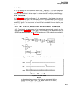
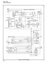
4-79. TIME BASE
4-80. The 5328A Time Base circuit is comprised of an 8-decade divider U21, shaping flip-flop
U19A, and Synchronization flip-flop U19B. The Time Base input, depending on the particular
measurement being made, is either the 10 MHz system clock or the Channel A or B input signal.
These signals are routed to the Time Base input via the ROM-controlled Time Base Multiplexer,
U10 on the A4 Function Selector board.
4-81. The Time Base circuit has two modes of operation consistent with the two types of mea-
surements performed by the 5328A. For frequency and time interval type measurements, the
Time Base circuit generates a gate during which either oscillator or input pulses are counted.
For totalize type measurements, the Time Base circuit divides its input by N as set on the
RESOLUTION, N switch on the front panel and outputs the divided signal to be counted in the
DCA. The outputs of the Time Base circuit, corresponding to both operating modes, are gener-
ated simultaneously. Regardless of the type of measurement being performed, these outputs
are made available to the A4 Function Selector which selects the proper signal to perform the
function.
4-82. The length of the gate time generated by the Time Base circuit and the scale factor of
the Time Base Input is determined by the Time Base code. The 5328A Mainframe ROM reads
the codes of both the Time Base (RESOLUTION, N) and FUNCTION switches and outputs the
proper code to the Time Base such that measurement resolution and scale factor agree with
the information in the various (RESOLUTION, N) switch positions.
4-83. A2 POWER SUPPLY
4-84. The power supply has five output voltages: +5, -5.2, +15, -15, and +3.5 volts, dc. The
+5V and -5.2V circuits are essentially the same as are the +15V and -15V sections, so only the
positive voltage sections will be described.
4-85. +5V Supply
4-86. The +5V supply is a switching regulator that has greater efficiency than a linear regu-
lator of the same output, When the output voltage is below its nominal level, comparator U1 sees
its + input being above its -
input and hence its output goes positive turning on transistor Q5
which in turn turns on Q3 and Q1. The voltage at the collector of Q1 now goes high (greater than
17V) and current starts to build up through L1, charging the output capacitor and increasing
the output voltage. At the same time positive feedback is provided via resistor R11 to maintain
the situation until the output goes slightly above +5V. When the voltage reaches this point the
comparator output voltage starts to fall turning off transistors Q5, Q3, and Q1 causing the volt-
age at the collector of Q1 to fall. This provides positive feedback via resistor R11 to reinforce
the charge. As a result, transistors Q5, Q3, and Q1 are turned off hard, and the voltage at the
collector of Q1 goes negative, except for diode CR3 which clamps the voltage to ground. During
this part of the cylce, current flows through diode CR3 and coil L1 allowing the energy which
has been stored in the field of L1 to go into the load. This goes on until the output voltage again
goes low enough to overcome the offset at the input of comparator U1 and turn transistor Q1
on again.
4-11