


Model 5328A
Maintenance
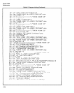
5-51. Programming Logic Troubleshooting includes Tables 5-12 and 5-13. Table 5-12 Program
Interface Operation shows the necessary levels that the A10 must generate in any function. Input
and Output codes for ROM (A10U7) are contained in Table 5-13.
5-52.
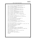
DAC Troubleshooting includes a checkout procedure that does not require a programming
source. Table 5–14 DAC Logic Levels gives the required logic output levels for proper operation.
The information in Table 5–15 DAC Signals is designed to aid in troubleshooting. It should be
used to troubleshoot problems where the logic levels are correct, yet the analog output is bad.
5-53. DAC TROUBLESHOOTING. To perform DAC troubleshooting proceed as follows:
a.
Check +5, -5.2, +15, and -15 volts on the A1 Motherboard (refer to A1 troubleshooting
procedure for repair).
b. Check for clock signal on U5 pins 8 and 11 and on collector of Q7. If incorrect, suspect
U5, Q7, or C12.
c.
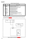
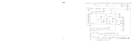
Perform the following setup procedure:
1.
Turn 5328A power off and unplug 14-conductor cable from A11J1.
2.
Remove DAC board A11 from 5328A and install jumpers in J1 from pins 8 to 10,
5 to 6, 4 to 7, and 3 to 12. Reinstall All board using an extender board (05328-
62016) into XA11.
NOTE
Ensure jumper from pin 8 to 10 does not short to any of the
other jumpers.
3.
Apply power to an HP 10526T Logic Pulser.
4.
Connect HP 3490A Voltmeter between A11TP5 and 5328A chassis (used to
monitor Channel A DAC output).
5.
Turn 5328A power switch to ON.
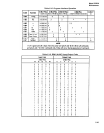
d. Pulse A11U11 (14) with the logic pulser. This resets the DAC storage registers. HP 3490
Voltmeter should display OV ±50 mV. If so, perform step 5. If not, refer to Table 5-14 and
check the logic levels listed on line 1 (reset pulse U11(14)) for an improper level. Sus-
pect any integrated circuit listed if it has an improper output.
e.
Pulse A11J1(14) once with the logic pulser and verify line 2 of Table 5–14.
f. Pulse A11J1(14) three more times, stopping after each pulse to verify the next line of
Table 5-14.
g. Steps a through f have checked the A channel DAC. To check the B channel DAC change
the voltmeter connection to A11TP6 and 5328A chassis. Repeat steps d through f,
pulsing A11J1 pin 13 instead of pin 14. The parentheses in Table 5-14 refer to B channel
DAC circuit locations.
h. If the A and B channel DAC output voltages were the same as in Table 5-74 the board
is functioning correctly. If a digital output from Table 5–74 is incorrect, suspect the
integrated circuit generating the level. If the digital outputs are correct and the analog
output is incorrect continue with step i.
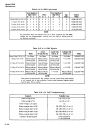
i. Reset storage registers (U16, U15, U11, U10) by pulsing A11U10(14) with a logic pulser.
Using an oscilloscope check signals listed in line 1 of Table 5-15.
j
Pulse A11J1(14) and again using the oscilloscope check for signals in line 2 of Table 5–15.
k. Pulse A11J1 (14) three more times, stopping after each pulse to verify the next line in
Table 5–15 with the oscilloscope.
l. Sets i through k have checked the A channel DAC signal path. To check Channel B
DAC, follow steps i through k above, pulsing A11J1 pin 13 instead of 14. Stop after each
pulse to verify the locations in parentheses of Table 5-15.
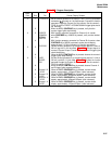
m. Refer to Table 5-16 match the symptom received with the probable cause of trouble.
5-42