


Model 5328A
Theory of Operation
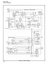
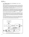
4-114. The A11 DAC board processes the four serial data bytes, and produces one parallel
BCD output. The BCD output provides the information for generating a square wave train by
using a series of rate multipliers. The square wave train has an average duty cycle proportional
to the input code supplied to the rate multipliers. This square wave train switches on a pre-
cision current source that feeds a voltage averager to produce a dc output.
4-115. REMOTE CONTROLLABLE (PROGRAMMABLE)
INPUT SCHEMATIC THEORY
4-116. Theory of operation for the programmable input section is given in the following
paragraphs.
4-117. A19 Switch Control Board
4-118. In local mode, -0.7 volts is applied to switches S1-S8. This potential allows the switches
to control their respective functions by supplying an active low available at each switch. In a
closed switch position, the -0.7 volts will forward-bias the associated diode, pull the anode low,
and cause a low to be sent to the amplifier board through J3.
4-119. In remote mode, the -0.7 volts switches to +5 volts, only allowing the output lines, trans-
mitted through J3, to be high. When a switch is open, the pull-up resistor on the line causes it
to go high. When the switch is closed, the associated diode is reverse biased and the line re-
mains high,
4-120. Trigger LEDs, DS1 and DS2, are driven by the inverted A and B outputs of the Schmitt
trigger (A12U4). These signals enter pins 14 and 10 of ECL-to-TTL translator U1. Feedback
capacitors C8 and C9 stretch the 5 nanosecond ECL pulse to approximately a 25 millisecond
TTL output pulse. This 25 millisecond pulse is of long enough duration to be seen, and is used
to drive the trigger LEDs. Since this pulse stretcher is decoupled to the Schmitt trigger, it functions
like a logic probe with adjustable threshold voltage. When Channel A input is higher than the
trigger level setting, the trigger LED is ON. When the input is lower, the LED is OFF, and when-
ever it passes through the trigger threshold, the LED flashes on or off depending on the polarity
of the input signal.
4-121. The 5 nanosecond inverted A and B outputs are also applied to pins 2 and 6 respectively
of U1. The signals are translated from ECL to TTL levels and connected to the marker outputs.
4-122. A12 Amplifier Board
4-123, Since both A and B channel circuitry are identical only the A channel will be discussed.
4-124. Input signal A enters A12 through J2 and depending on relay K7 is either ac coupled
through capacitor c30 or dc coupled across relay K7. The signal then enters the three position
attenuator (X1, X10, X100) and is passed from the selected attenuation node through either K2,
K3, or K8 to the input of the FET impedance converter stage. Diodes CR5 and CR6, resistors R39,
R37, and R34, and capacitors C23 and C24 form an overvoltage protection network to limit the
signal sent to FET transistor Q3 and successive circuits to ±2.61 volts maximum, The signal at
the node between resistors R30 and R32 follows closely the signal at the gate of Q3A. A poten-
tiometer is used to adjust any initial offset voltage.
4-125. SEP/COM A relays, K4 and K5, connect the input of the B channel attenuator to either
the A or B channel inputs. The signal then passes through U4, a dual Schmitt trigger, Trigger
U4B compares the signal at pin 9 to a dc reference between ±2.5 volts on pin 10. This dc reference
is selected by K1 and is supplied by either the A11 DAC board or by the A19Switch Control board.
The output of U4 changes state whenever the input crosses the reference voltage on U4(11).
The output is ECL (=-0.8 to -1.6V) and drives both the A trigger LED circuit on the A19 board
4-16