


Model 5328A
Theory of Operation
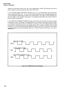
and the exclusive OR gate U2. Schmitt trigger U4 has approximately 15 mV peak-to-peak
hysteresis at its input. Exclusive OR gate U2 is used to select the desired slope of the input
waveform. When pin 7 of U2 is held to an ECL high level (SLOPE switch in + position), U2 acts
as an inverter. When pin 7 goes low (SLOPE switch in the - position), U2 does not invert the
signal passing through it.
4-126. Input signal conditioning control is accomplished by inverters U1 and U3 and relays
K1-K12. This control is supplied from either the A10Synchronizer board or the A19Switch Con-
trol board. When the 5328A is in remote, relay control is received through J1 from the A10 board,
In the local mode, relay control arrives via P2 from the A19 board. Since all of the relay control
lines contain inverters, relay activation is caused by a high at the input.
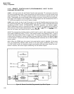
4-127. A10 Synchronizer Board
4-128. The differential A channel outputs from A12U2 feedthrough connector P2 pins 7 and
8 respectively to U1. Circuit U4 is a one-shot that only triggers on a negative edge, and therefore,
passes only trigger events that occur on the slope selected by A12U2. The output of U4 pin 15
is an ECL pulse of approximately 5-10 nanoseconds width. In the FREQ A check mode, the
oscillator signal from U1(2), (either 10 MHz or 100 MHz as selected by S1) is injected via U5B
to U10(13). The normal A input entering U10(12) is disabled at A12U4 by LCHK being low. The
oscillator signal at U10(13) is passed through U10C and U10D to U11 a dual 4 to 1 multiplexer.
In a noninverting mode, multiplexer U11 always routes the A channel signal to the start syn-
chronizer U6A. In a period function, U11 routes the A channel signal to the stop synchronizer
U6B. For time interval measurements, the B channel signal is supplied to stop synchronizer U6B.
ROM line R6 controls the stop synchronizer input switching. In remote, HINV, from U11(7)
allows the A and B channel outputs of U11 to be inverted. The outputs of U11A feed U12A
which drives the A and A outputs to the A4 Function Selector.
4-129. In Tl, TI AVG, PER, and PER AVG functions, U5, U6, U12, and U13 are used to gener-
ate synchronized time interval and gated oscillator pulses for the mainframe. After a reset pulse
arrives on the HDS line, the RS FFs US and U12 and D FFs U6A and U6B are reset. At the same
time, the and GOSC outputs are at an ECL high. When a start event enters U5D pin 12, it sets
the U5A output to U6A pin 7 high. The next clock pulse to U6(6) will cause U6A pin 3 to go low.
This pulls the output low, signaling to the function selector that the time interval has started,
When TI goes low, GOSC (U13B) starts to output oscillator pulses. When a stop event occurs
at U5(10), the output of U12C goes high. This, synchronous to the next clock pulse, sets U16(15)
high. When U16(15) goes high, the TI and GOSC outputs go high stopping the time interval
measurement. The Q output of U6B through U13C, U14B, and U14A resets all FFs and thus
prepares them for the next measurement.
4-130. ROM line RL6(HC), connected to U14(11) by R6, is used in period measurements. This
line is set low in period, and holds the stop FF (U5C and U12C) off until the start synchronizer
U6A clocks a high to its Q output.
4-131. In a PER AVG function where time base scaling takes place, ROM line RL5(T10) is
driven high. This TTL high is converted to an ECL high, by resistors R18 and R21, and applied
through U14D to U12(1)). This causes the stop synchronizer flip-flop (U5C and U12C) to remain
in a reset condition.
4-132. The programming interface has two operational modes, the non-DAC and DAC control
modes. These modes refer to the operation of the interface with respect to incoming data.
When the incoming data is for control of signal conditioning (not trigger level) the interface
will be in the non-DAC mode. The interface will be in the DAC control mode when incoming data
is for DAC (trigger level) control.
4-17