


Model 5328A
Theory of Operation
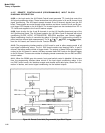
4-133. When the 5328A goes into remote, LEXT goes low. The low, on LEXT, causes the output
of A1 Motherboard switch control circuit to go from -0.7 volts to +5 volts. This change, disables
front panel switch control on the A16 and the A19 boards. When LEXT is low, U17(4) connected
to tri-state buffers U2 pin 1 and U9 pines 1 and 15 is also low. This low, returns the outputs of
tri-state buffers, U2 and U9, to their active state. With the outputs of U2 and U9 enabled, the
outputs of addressable latches, U8 and U15, control the A12 signal conditioning relays.
4-134. The interface is reset by a high on the HRPR line. This high is generated by the A15
HP-IB Interface Board when it receives an ASCII “P”.
4-135. When the interface is reset it defaults to the non-DAC control mode. The reset causes
the latched outputs of U8 and U15 to go low. This sets U17 pins 9 and 10 low, giving a low at
U17(8), The low at U17(8) is connected to U7(14), where it causes the interface to be in the non-
DAC mode. The low at U17(8) is also connected to clock multiplexer U16(1) where it causes U16
to route clock (LMS) pulses to only U8 or U15.
4-136. Clock multiplexer U16 decodes the MA and MB lines, from the A15 board, to determine
whether the input data byte, on MDA-MDD, is A or B channel information. It then routes the
clock pulse to U8(14) for A channel information, or to U15(14) for B channel information. The
clock pulse, latches the information into the intended latch.
4-137. After reset, the interface defaults to all of the underlined functions in Table 3-5 Pro-
gram Code Set. To change one of the signal conditioning controls it is necessary to program
that function.
4-138. As an example, assume a Channel A function setting of X1 is desired. This means that
an “A7” must be included in the data string sent by the system controller to the 5328A. When the
“A” is decoded by the A15 HP-IB interface, it causes the MA line to be high and the MB line to
be low. The MA and MB lines are decoded by U6 and it routes the following clock pulses to U8.
4-139. When the “7” is sent, 1110 appears at the input of ROM U7 on MDA-MDD respectively.
As shown in Table 5-28, the 1110 at the input causes an output of 000011 on U7 pins 1-6.
4-140. The clock pulse arrives at U8(14) and latches the high on U8(13) to U8(5). The high on
U8(5) is buffered by U9 and appears at pin 13 of its output. The high at U9(13) is inverted on the
same function as Channel A.
4-141. All non-DAC information is latched in the same manner. B channel information is
latched into the outputs of U15. it has the same code into U7, and thus the same code out of U7,
for the same function as Channel A.
4-142. Refer to Table 3-5 Program Code Set for the proper format to program a trigger level.
The proper format is ±X.YZ*, and follows an A and B which indicates to which channel it
applies.
4-143. For the following discussion, assume a trigger level is programmed, following the
proper format, and preceeded by an “A”,
The interface resets to the non-DAC mode when the
A15 board receives an ASCII “P” from the system controller. When the A15 board receives the
“A”, the MA line is set high and the MB line is set low. U16 decodes the MA and MB lines, in the
non-DAC mode, and clocks the A channel latch U8.
4-144. When a + or - appears on the MDA-MDD lines, a high is latched into U8(12), Latching
occurs on the positive clock pulse transition from U16. The high at U8(12), will cause U17(8) to
go high. U17(8) is connected to U7(14), where the high changes the input address to ROM U7,
and locks the interface into the DAC control mode. The high at U17(8) is also connected to
U16(1). A high at U16(1) causes U16 to supply clock pulses to either the A or B channel DAC.
4-18