


Model 5328A
Theory of Operation
the use of the letter “N” in a decision diamond symbol. ) The preset (jump) is synchronous and
only occurs when pin 9 of U14 and U23 is low and when there is a rising edge at pin 2 of U14
and U23. FF U31A synchronizes the reset of the State Counters to occur at the proper time.
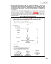
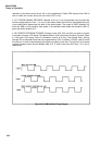
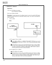
4-190. ASM OSCILLATOR. As shown in the ASM Oscillator Timing Diagram, Figure 4-70,
the ASM oscillator circuit provides three separate phases of clock outputs. Schmitt trigger
U18A is the fundamental oscillator element which uses hysteresis to develop oscillation, The
output of U18A (through U13) strobes storage latches U11A and B, U15, U19, U24, U26, U28,
U33, U31B, and U34. The output of U18A is also sent through a delay circuit consisting of re-
sistor R14 and capacitor C4 into U18B to provide another phase of the clock output that deter-
mines the next state of the ASM. In addition, the output of U18A is sent through U30A to pro-
vide a third clock phase which is applied to U31A. The output of U31A resets the 8-bit State
Counter synchronously at power up or when the IFC signal occurs. (Synchronous reset prevents
loading the storage latches with erroneous data.) The IFC signal also resets U26 (ASM storage).
The power up reset circuit U18C and U18D clears all storage elements.
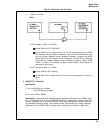
4-191. BUS INTERFACE. The bus interface circuit consists of bus line termination resistors,
data output drivers and data input buffers. Resistors R29 and R30 form the line termination net-
works, U4 is used to buffer the bus line inputs and U5, U10, and U16 are high current drivers
that drive the bus lines output. The ATN signal is sent through U9A and U29D to ensure that
the gates connected to bus lines DIO1—DIO7 and DAV do not output when ATN goes true. The
DAO signal from U24(9) arms the DAC signal through U17B to ensure that DAC goes false
within a few gate delays after ATN goes true. (1 n some cases, the DAC response from the ROM
may be too slow.) After ATN is true, DAO is set to a “0” to allow normal operation of the DAC
line.
4-192. END OF MEASUREMENT. When a measurement has been completed, FF U11B is set.
This FF is clocked by the closing edge of the LMG signal. Diode CR2 and transistor Q3 keep U11B
from going to the “l” state when LRES is low or HRD is high, (During these times the counter
is being reset and noise appears on the LMG line which could trigger UIIB.)
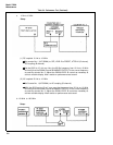
4-193. QUALIFIER MULTIPLEXER. Five 8-to-1 multiplexer are connected to allow 36 lines
to be multiplexed into 1 line. ASM ROM U22 controls multiplexer U3, U6, U8, and U32 to
select individual line qualifiers and U12 to select one of these multiplexer. In addition, U12
checks the output of auxiliary State Counter U7, a 4-bit binary counter that allows the same
sequence of states to be repeated up to 16 times. In the output algorithm, each state represents
an output character. Qualifier FF U11A eliminates erroneous results by ensuring that the State
Counters U14 and U23 are not clocked when a qualifier is changing states. This would cause a
partial preset and partial increment of the State Counters,
4-194. ADDRESSING. Address Comparator U2 monitors the Data Input/Output (DIO) lines
2 through 5 and the address switch (S1) settings. When a comparison occurs between the state
of these DIO lines and the address switch settings, U2 sends qualifier ADDR to multiplexer U8.
The TALK ALWAYS section of the address switch provides a means of setting U6 so that inter-
face is always addressed to talk.
4-195. DATA OUTPUT. The Data Output circuit outputs characters on the bus data lines.
Storage circuit U24 transfers outputs from the ROM to DIO lines 5 through 7. U15 selects data
from either the ROM or the 5328A data bus and transfers it to DIO1—DIO4. The state of the “not”
bit from ROM U22(13) through U21E determines the selection made by U15. A displayed digit
is selected from the 5328A, any other characters (decimal point,
“E”, carriage return, exponent,
linefeed, etc.) are selected from the ROM.
4-196. ASM STORAGE. The internal memory for the ASM operation is in ASM Storage circuits
U19, U26, and U31B. There are 17 information bits that can be set or cleared by these circuits.
This section also includes one-shot U1 which outputs a 2 ms pulse (LRST) to ensure reliable
4-23