


Model 5328A
Theory of Operation
4-87. +15V FAN POWER. The +15V supply is a simple linear regulator using transistor Q7 as
the pass transistor. Transistor Q2 provides level shifting and current gain while U3 is used as
comparator and gain block. The 5328A cooling fan motor receives power from A20. A20 is a
sealed unit which produces an alternating current from +15 volts input.
4-88. The +3.5V supply is also a simple linear regulator with the operational amplifier section
of U5 being used as a comparator and gain block. Resistor R32 provides overcurrent limiting to
protect against shorts.
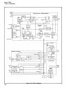
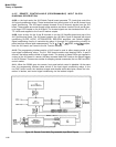
4-89. A4 FUNCTION SELECTOR
4-90. The A4 Function Selector serves as the main high-speed switching module of the 5328A.
It receives high-speed differential ECL data from the Main Bus (from the modules that process
the signal input) and routes that data to either the Time Base or the DCA. In addition, the Main
Gate FF, the Arming Multiplexer and Arming FF, and the First Decade of the DCA are on the
A4 Function Selector assembly.
NOTE
Refer to Table 8-7 for definitions of mnemonics.
4-91. High Speed Multiplexer, Main Gate, and 1st Decade
4-92. High speed multiplexer U6 serves as the main multiplexer and routes the following
signals to the 1st decade of the DCA: A, B, GATES OSC (GOSC), C, DVM, TIME BASE OUT
(TBO), and OSCILLATOR (OSC). ROM lines IA, IB, and IC control the active address of the
multiplexer. Pin 2 (enable) of the multiplexer serves as the Main Gate. The Low Time Interval
(LTIF), Low Main Gate FF (LMGF), or (LTOTŽLST), signal operating through U8 and enabled
by ROM lines LMGF, LTIF, (LTOTŽLST), respectively control the Main Gate. In addition,
ROM line HOPN can override LTIF or LMGF and lock open Main Gate U6(2) through U8C. Main
Gate status is detected and sent off the A4 Function Selector by ECL-to-TTL translator U2D.
Capacitor C11 and resistor R35 serve to stretch any ECL gate signal present at U2(10) so that
the slower TTL control chip A1U4 and gate light one-shot
(Q6, U36B, E) can see the pulses and
properly react. U8D differentially drives bus lines MG and M to operate the remote Main Gate
of Channel C.
4-93. The output of the main multiplexer U6(15) feeds into first binary U1 of the main DCA.
U1A is an ECL High-Speed binary the output of which couples to pins 14 and 15 of ECL-to-TTL
translator U2. The TTL output of U2(13) clocks Schottky quinary U4 and U3. The outputs of the
first decade U3(9), U4(9), U3(5), and U2(13) travel off the A4 Function Selector board to the
DCA on the Al Motherboard where they are latched and the carry feeds into the next decade of
the DCA.
4-94. Arming Multiplexer and Arming FF
4-95. The Arming FF, the second half of U4, serves to inhibit various measurements by en-
abling or disabling Time Base Multiplexer U10 and the synchronizers in the Universal Module.
This action occurs via the High Disables Syncrhonizers (HDS) signal from U4(6). The signal
which sets or enables U4 comes from Arming Multiplexer U5(6). ROM lines control U5(10, 11)
while the remaining address line (pin 9) is controlled by the Low Arm (L ARM) signal from the
rear panel ARM switch. US thus selects either C-ARM, B, B, or free run (+5V) as the signal to
send to U4 as the Arming signal. The A and B signals are derived from ECL-to-TTL translator
U2A and U2B, respectively. Capacitors C4 and C5 and resistors R17 and R18 serve as pulse
stretcher timing elements to enable the narrow ECL pulses on lines
~
and
~
to be seen by the
TTL Arming FF U4.
4-12