


Intel
®
82854 Graphics Memory Controller Hub (GMCH)
100 D15343-003
4.11 Intel
®
82854 GMCH Integrated Graphics Device Registers
(Device #2, Function #0)
This section contains the PCI configuration registers listed in order of ascending offset address.
Device #2 incorporates Function #0. See “Nomenclature for Access Attributes” on page 42 for
access nomenclature.
Note: C0F0 = Copy of Function #0 and U1F1 = Unique in Function #1.
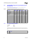
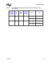
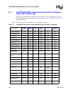
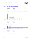
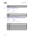
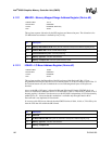
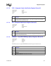
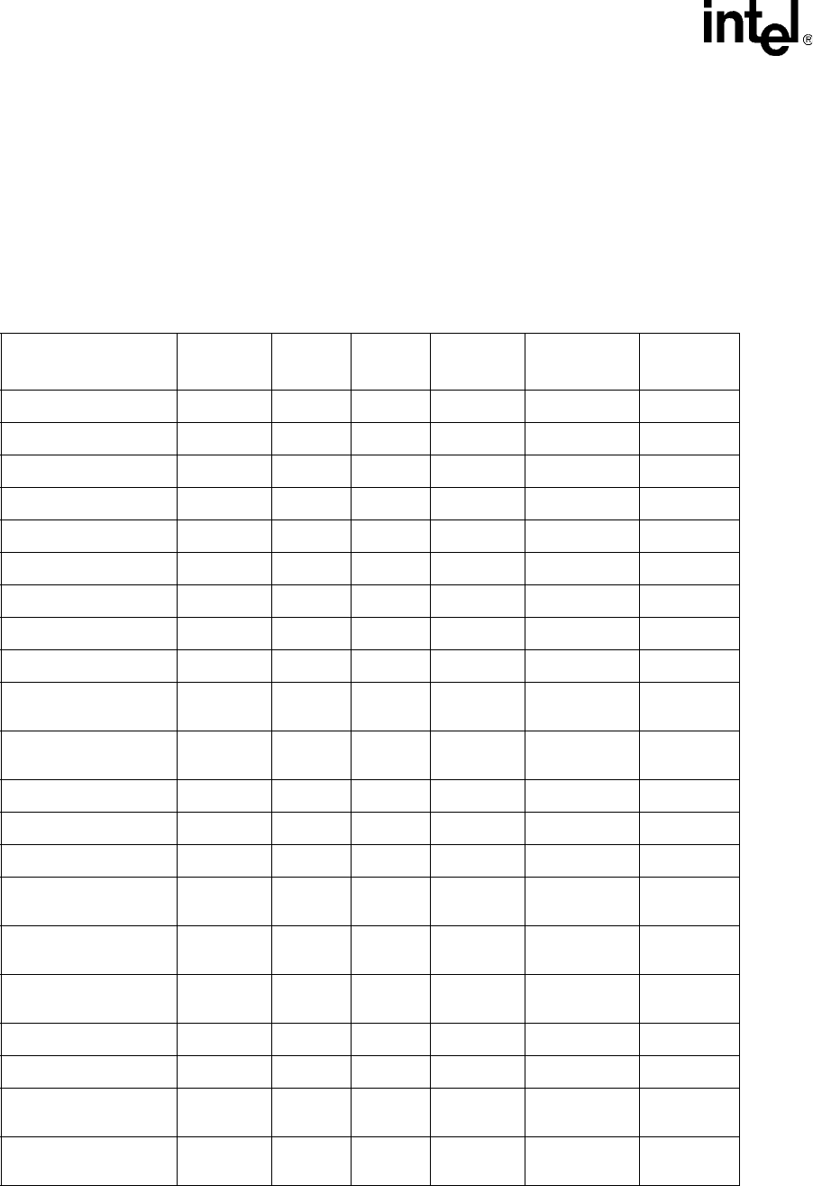
Table 25. Integrated Graphics Device Configuration Space (Device #2, Function#0)
Register Name
Register
Symbol
Address
Offset
Register
End
Default
Value
Access
Regs in
Function#1
Vendor Identification VID 00h 01h 8086h RO C0F0
Device Identification DID 02h 03h 358Eh RO C0F0
PCI Command PCICMD 04h 05h 0000h RO,R/W U1F1
PCI Status PCISTS 06h 07h 0090h RO U1F1
Revision Identification RID 08h 08h 02h RO C0F0
Class Code CC 09h 0Bh 030000h RO U1F1
Cache Line Size CLS 0Ch 0Ch 00h RO C0F0
Master Latency Timer MLT 0Dh 0Dh 00h RO C0F0
Header Type HDR 0Eh 0Eh 00h RO C0F0
Graphics Memory
Range Address
GMADR 10h 13h 00000008h RO,R/W U1F1
Memory Mapped Range
Address
MMADR 14h 17h 00000000h RO,R/W U1F1
IO Range IOBAR 18h 1Bh 00000001h RO,R/W –
Subsystem Vendor ID SVID 2Ch 2Dh 0000h R/WO C0F0
Subsystem ID SID 2Eh 2Fh 0000h R/ WO C0F0
Video Bios ROM Base
Address
ROMADR 30h 33h 00000000h RO C0F0
Interrupt Line INTRLINE 3Ch 3Ch 00h RO in F#1,
R/W
–
Interrupt Pin INTRPIN 3Dh 3Dh 01h RO, Reserved
In F#1
–
Minimum Grant MINGNT 3Eh 3Eh 00h RO C0F0
Maximum Latency MAXLAT 3Fh 3Fh 00h RO C0F0
Power Management
Capabilities
PMCAP D2h D3h 0221h RO C0F0
Power Management
Control
PMCS D4h D5h 0000h RO,R/W U1F1